Edge termination configurations for high voltage semiconductor power devices

a technology of high-voltage semiconductor and termination configuration, which is applied in the direction of semiconductor devices, semiconductor/solid-state device details, electrical apparatus, etc., can solve the problems of increasing difficulty, limiting difficulty, and terminal area still faced, so as to reduce the crowding effect of electrical fields, solve problems and difficulties, and reduce the effect of high breakdown voltag

Active Publication Date: 2014-02-04
ALPHA & OMEGA SEMICON INC
View PDF5 Cites 8 Cited by
  • Summary
  • Abstract
  • Description
  • Claims
  • Application Information

AI Technical Summary

Benefits of technology

[0009]It is therefore an aspect of the present invention to provide a new and improved edge termination configuration to reduce the electrical field crowding effects in the termination area such that the required area in the edge termination can be reduced while achieving high breakdown voltage thus resolving the problems and difficulties as that encountered in the conventional technologies.
[0010]Specifically, an aspect of this invention is to provide a new and improved edge termination configuration that can effectively move the peak electrical field point into a region laterally away from a P body region thus making the potential lines flatter in the silicon thus reducing the electric field crowding and significantly increases the breakdown voltage without requiring large termination area.
[0011]It is another aspect of this invention to provide the new and improved edge termination configuration by forming a wide oxide trench with a buried field plate extends laterally along a top part of the oxide trench, proximity to the P body region, such that the peak electrical field is laterally moved away from the body region thus reduces the field crowding effect and increasing the breakdown voltage while reducing the required area of the edge termination.

Problems solved by technology

Conventional manufacturing technologies and device configuration to further increase the breakdown voltage of a semiconductor power device at the terminal areas are still confronted with difficulties that the termination areas occupy large areas.
The difficulties are becoming more severe and limiting especially when the semiconductor power devices are now manufactured with ever reduced size.
The termination area is a “non-active” area of a transistor because the edge terminal is not useful for current conduction.
Even though large areas taken up by the edge termination leads to wastes of valuable active cell areas there is still no viable solution to overcome this difficulty.
However, the actual breakdown voltage of a reversed bias junction can be severely degraded at the edge, due to field crowding from the formation of a cylindrical junction, as shown in FIG. 1B.
However, these methods typically require large area for implementation, and cause an increase in the die size of the device.
In addition, these techniques are prone to surface charges coming from the passivation films and / or the packaging mold compound.

Method used


Image

  • Edge termination configurations for high voltage semiconductor power devices
  • Edge termination configurations for high voltage semiconductor power devices
  • Edge termination configurations for high voltage semiconductor power devices

Examples


Embodiment Construction

Introduction

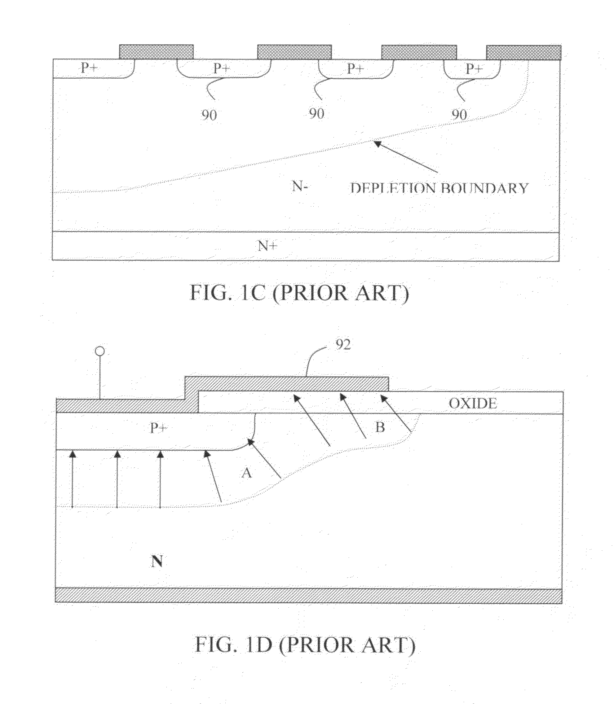
[0023]In order to overcome this electrical field crowding phenomena, a deep and narrow oxide trench 104 as that shown in FIG. 2A is attempted. In this approach, a deep oxide trench 104 is formed in the lightly doped N-type drain drift layer 101 adjacent to the P body region 102 with a width of the trench 104 is about five microns. Even that the deep oxide trench of five microns width is theoretically sufficient to block a voltage of 700 volts, the deep oxide trench 104 as shown in FIG. 2A, however, is not effective to increase the breakdown voltage beyond a range of 250 volts to 300 volts. The reason that the deep oxide trench 104 is not effective is due to the fact that the width of the oxide trench is not wide enough to flatter the electrical potential lines, which causes the potential lines bending ninety degrees from the silicon to the oxide trench with the peak electric filed point at the silicon region, not in the oxide region. The bending of the electrical potenti...


PUM


Abstract

This invention discloses a semiconductor power device disposed in a semiconductor substrate and having an active cell area and an edge termination area wherein the edge termination area comprises a wide trench filled with a field-crowding reduction filler and a buried field plate buried under a top surface of the semiconductor substrate and laterally extended over a top portion of the field crowding field to move a peak electric field laterally away from the active cell area. In a specific embodiment, the field-crowding reduction filler comprises a silicon oxide filled in the wide trench.

Description

BACKGROUND OF THE INVENTION[0001]1. Field of the Invention[0002]The invention relates generally to the semiconductor power devices. More particularly, this invention relates to configurations and methods to improve the termination regions of a semiconductor power device for reducing the areas occupied by the termination areas while maintaining high breakdown voltages for the high voltage power devices.[0003]2. Description of the Prior Art[0004]Conventional manufacturing technologies and device configuration to further increase the breakdown voltage of a semiconductor power device at the terminal areas are still confronted with difficulties that the termination areas occupy large areas. The difficulties are becoming more severe and limiting especially when the semiconductor power devices are now manufactured with ever reduced size. A general survey discovers that for smaller chips, the edge termination area takes up about 20% of the total area. However, as size of the chip becomes sm...

Claims


Application Information

Patent Timeline
Patent Type & Authority Patents(United States)
IPC IPC(8): H01L31/113H01L29/76H01L31/062H01L29/94H01L23/58
CPCH01L29/7811H01L29/41741H01L29/0661H01L29/407H01L29/41766H01L29/66727H01L2924/0002H01L2924/00
Inventor BOBDE, MADHURLUI, SIK KBHALLA, ANUP
Owner ALPHA & OMEGA SEMICON INC
Why Eureka
Try Eureka