
Volatile Memory with a Decreased Consumption and an Improved Storage Capacity

Active Publication Date: 2013-08-08
STMICROELECTRONICS SRL
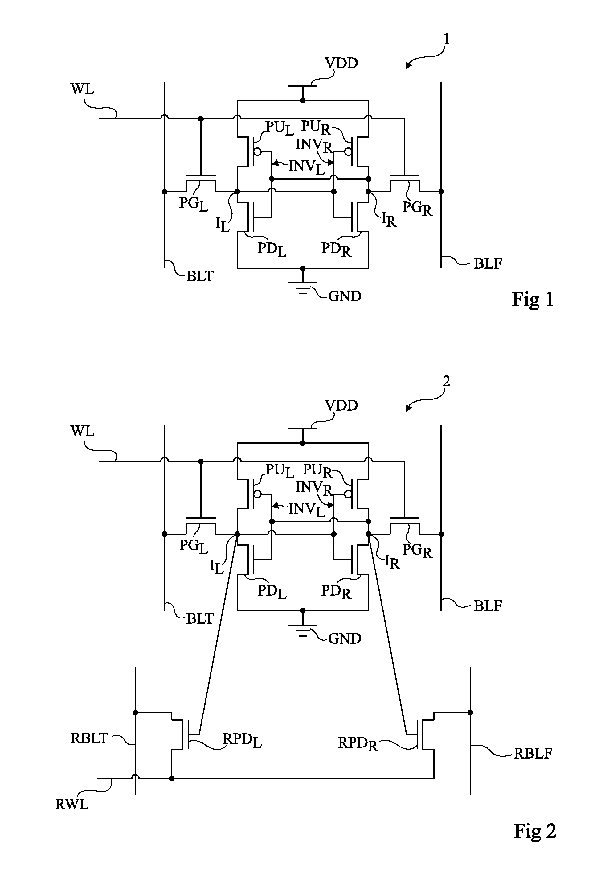
View PDF8 Cites 9 Cited by
  • Summary
  • Abstract
  • Description
  • Claims
  • Application Information

AI Technical Summary

Benefits of technology

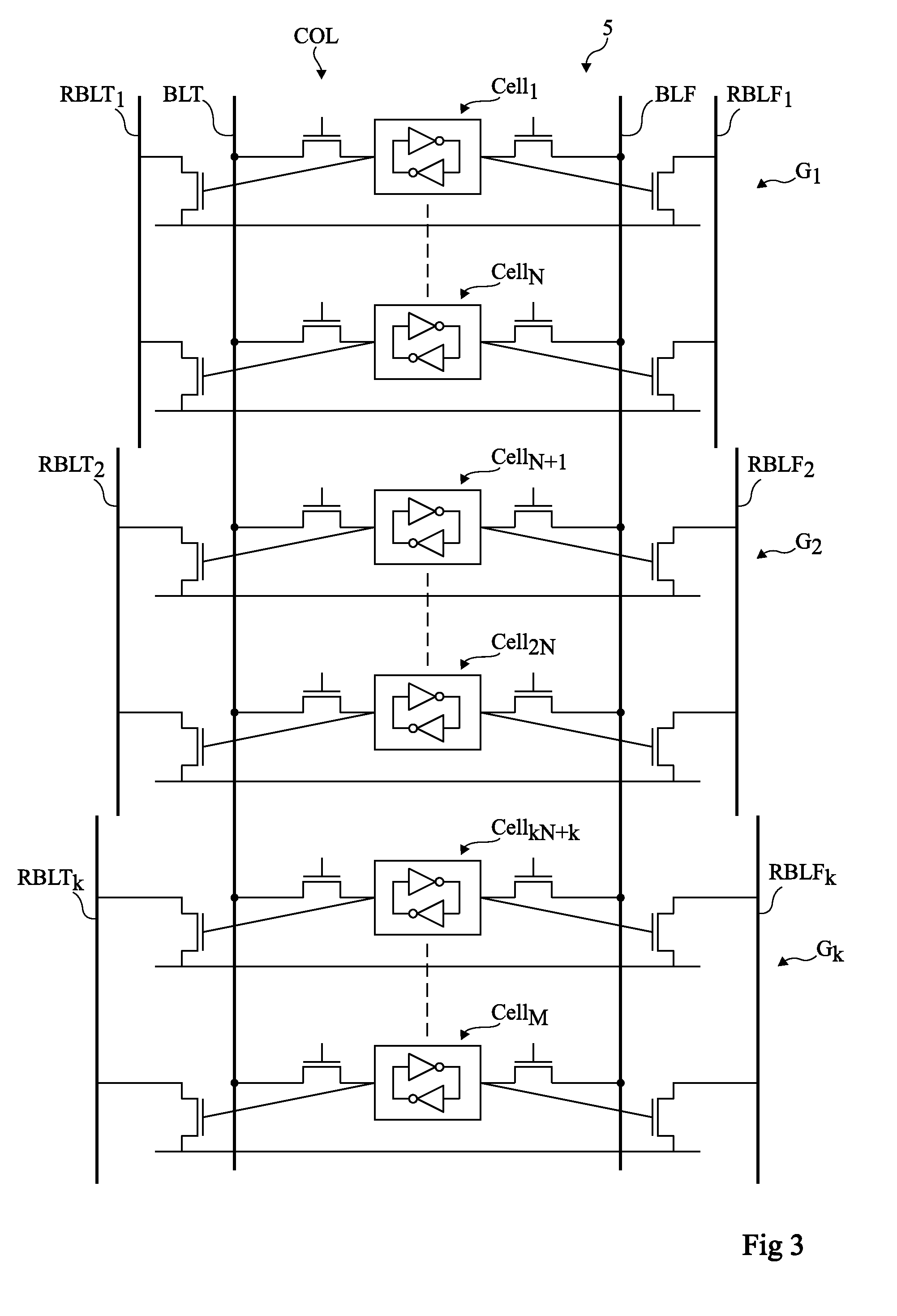
This patent describes a type of memory that uses less power and takes up less space than existing memories. The memory cells are organized in rows and columns, and each column has its own dedicated read and write bit lines. The memory cells are also distributed in two groups for each row, with one group dedicated to read operations and the other dedicated to write operations. Each memory cell has two inverters and a MOS transistor for writing and reading data. The first selection circuit can activate either the read or write bit lines for each column. The memory cells are connected to the read bit lines through a multiplexer and an amplifier. The patent also describes an electronic device that includes a battery and a memory.

Problems solved by technology

A memory is called volatile in the case where the data stored in the memory cells risk being lost when the memory power supply voltage falls below a minimum threshold.
However, some constraints may limit the maximum possible number of memory cells per column.
The larger the bit line capacitance, the more the bit line charge / discharge operation takes time during the read / write operation, which causes a decrease in the memory operating frequency.
For some applications, the consumption of the integrated circuit comprising a volatile memory is a critical factor.
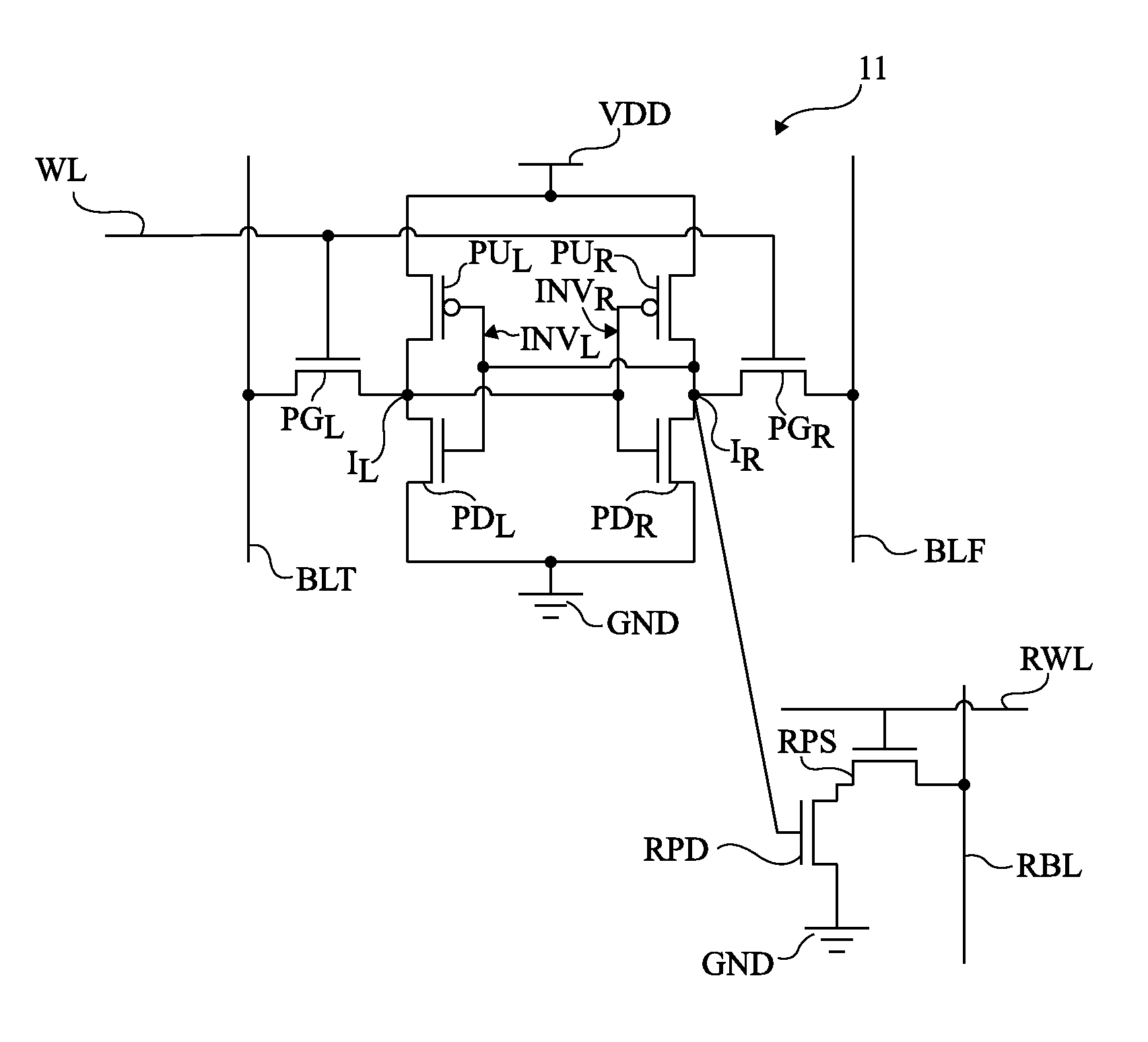
However, even if switches PGL and PGR of all the other memory cells of the column are on, leakage currents may flow for these memory cells through some of switches PGL and PGR.
Incorrect variations of the voltages of bit lines BLT and BLF, and thus read errors, may thus occur.
Further, even though transistors RPDL and RPDR may be designed to have decreased leakage currents in an operation of reading of the datum read from a memory cell of a column, the leakage currents of the unaddressed memory cells of the same column may disturb the read datum if the ratio of the read current (Tread) to the sum of the leakage currents (Ileakage) is too small, for example, smaller than 10.

Method used


Image

  • Volatile Memory with a Decreased Consumption and an Improved Storage Capacity
  • Volatile Memory with a Decreased Consumption and an Improved Storage Capacity
  • Volatile Memory with a Decreased Consumption and an Improved Storage Capacity

Examples


Embodiment Construction

[0051]For clarity, the same elements have been designated with the same reference numerals in the different drawings. In the following description, expression “conduction terminal” of a MOS transistor indifferently designates the MOS transistor source or drain.

[0052]The embodiments described hereafter may be implemented with a memory cell comprising read bit lines dedicated to read operations and separate from the write bit lines. In this type of cells, the read and write paths are separate.

[0053]As an example, the present embodiment may be implemented with the memory cell example described in FIG. 2. However, the embodiment of the present invention may be implemented in other examples of memory cells, and especially the memory cells described in publication “A 0.5-V 25-MHz 1-mW 256-Kb MTCMOS / SOI SRAM for Solar-Power-Operated Portable Personal Digital Equipment-Sure Write Operation by Using Step-Down Negatively Overdriven Bitline Scheme” by Nobutaro Shibatao, Hiroshi Kiya, et al. (I...


PUM


Abstract

A volatile memory includes volatile memory cells in which data write and read operations are performed. The memory cells are arranged in rows and in columns and are distributed in first separate groups of memory cells for each column. The memory includes, for each column, a write bit line dedicated to write operations and connected to all the memory cells of the column and read bit lines dedicated to read operations. Each read bit line is connected to all the memory cells of one of the first groups of memory cells. Each memory cell in the column is connected to a single one of the read bit lines.

Description

[0001]The present invention claims priority to French patent application 1251037, filed Feb. 3, 2012 and incorporated herein by reference.TECHNICAL FIELD[0002]The present disclosure relates to integrated circuits comprising volatile memory elements.BACKGROUND[0003]An integrated circuit memory may be formed of an assembly of memory elements, or memory cells, which may be arranged in an array. The writing and reading of data in memory cells are performed by dedicated logic circuits. A power supply generally provides the power necessary to the proper operation of the memory cell components and of the logic circuit. The memory power supply is generally obtained over one or several rails connected to all the memory cells and transmitting a power supply voltage. A memory is called volatile in the case where the data stored in the memory cells risk being lost when the memory power supply voltage falls below a minimum threshold.[0004]FIG. 1 shows an example of a volatile memory cell 1 of a ...

Claims


Application Information

Patent Timeline
IPC IPC(8): G11C7/10G11C7/00
CPCG11C7/00G11C7/10G11C8/16G11C8/12G11C8/14G11C7/18
Inventor FEKI, ANIS
Owner STMICROELECTRONICS SRL
Learn More