Programmable transceiver circuit

a transceiver and circuit technology, applied in logic circuits, logic circuit coupling/interface arrangements, pulse techniques, etc., can solve the problems of large silicon chip area, long signal delay, cost and time-consuming to customize each and every i/o buffer,

Active Publication Date: 2013-08-15
BAE SYST INFORMATION & ELECTRONICS SYST INTERGRATION INC
View PDF1 Cites 10 Cited by
  • Summary
  • Abstract
  • Description
  • Claims
  • Application Information

AI Technical Summary

Problems solved by technology

Suffice to say, it can be very costly and time-consuming to customize each and every I/O buffer for every application.
Such designs tend...

Method used


Image

  • Programmable transceiver circuit
  • Programmable transceiver circuit
  • Programmable transceiver circuit

Examples


Embodiment Construction

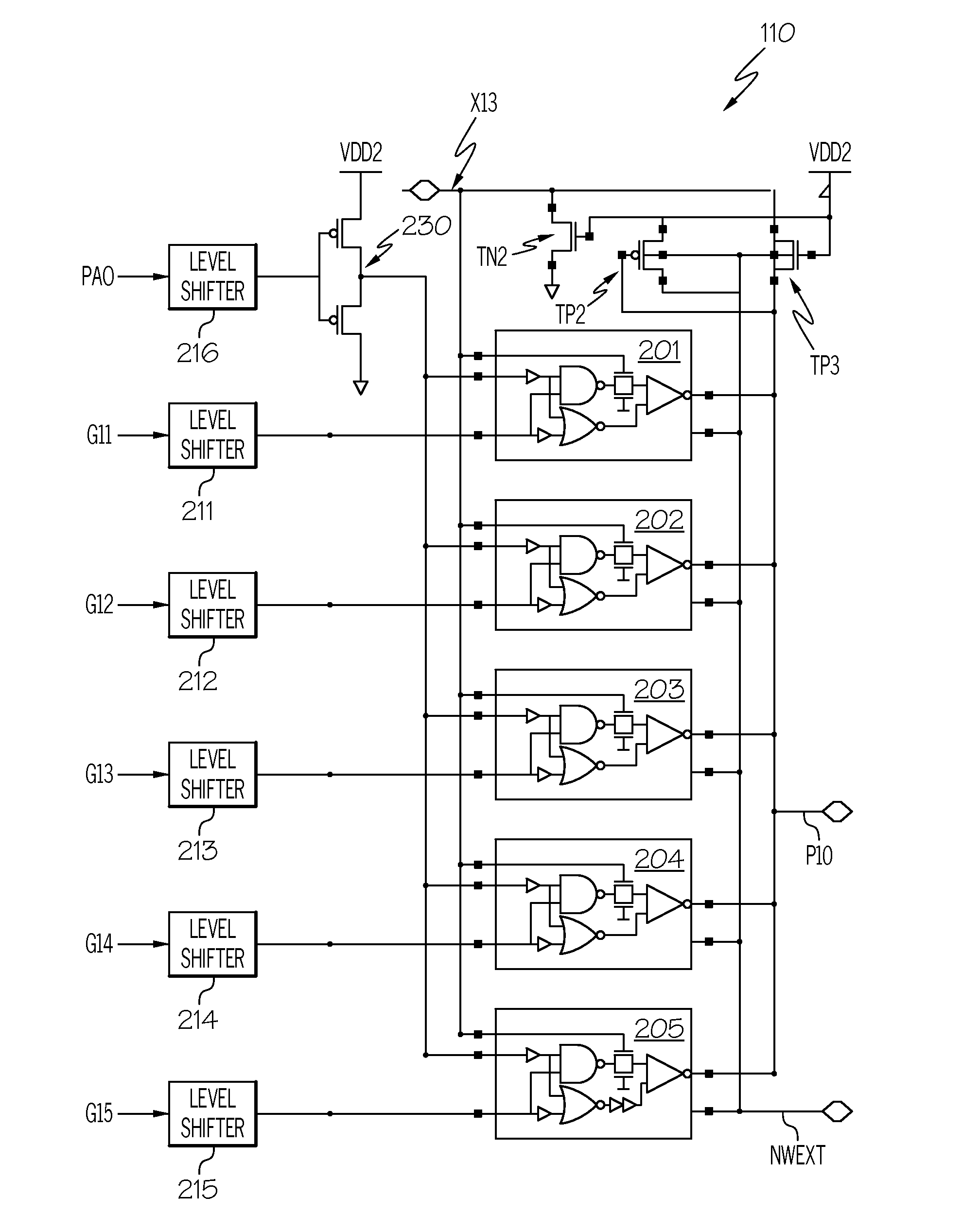
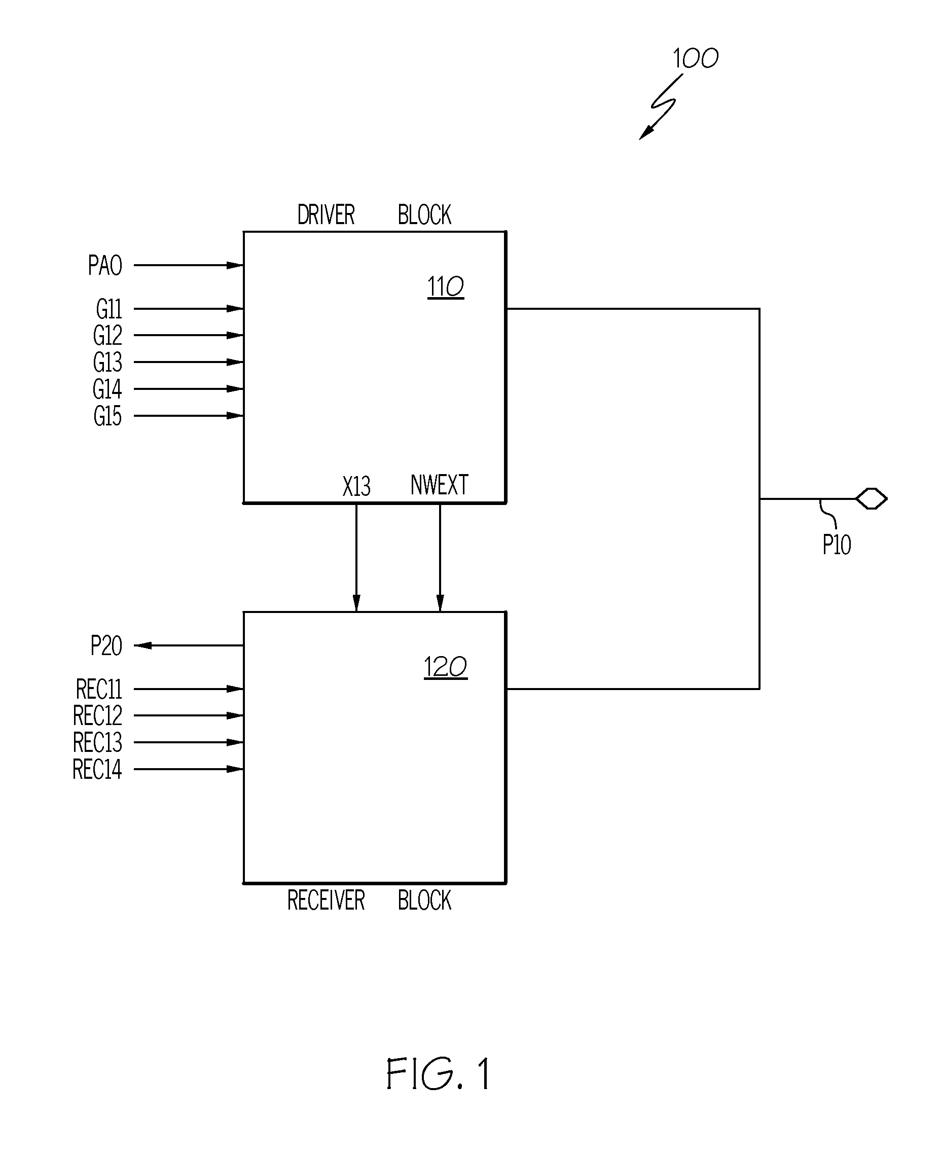
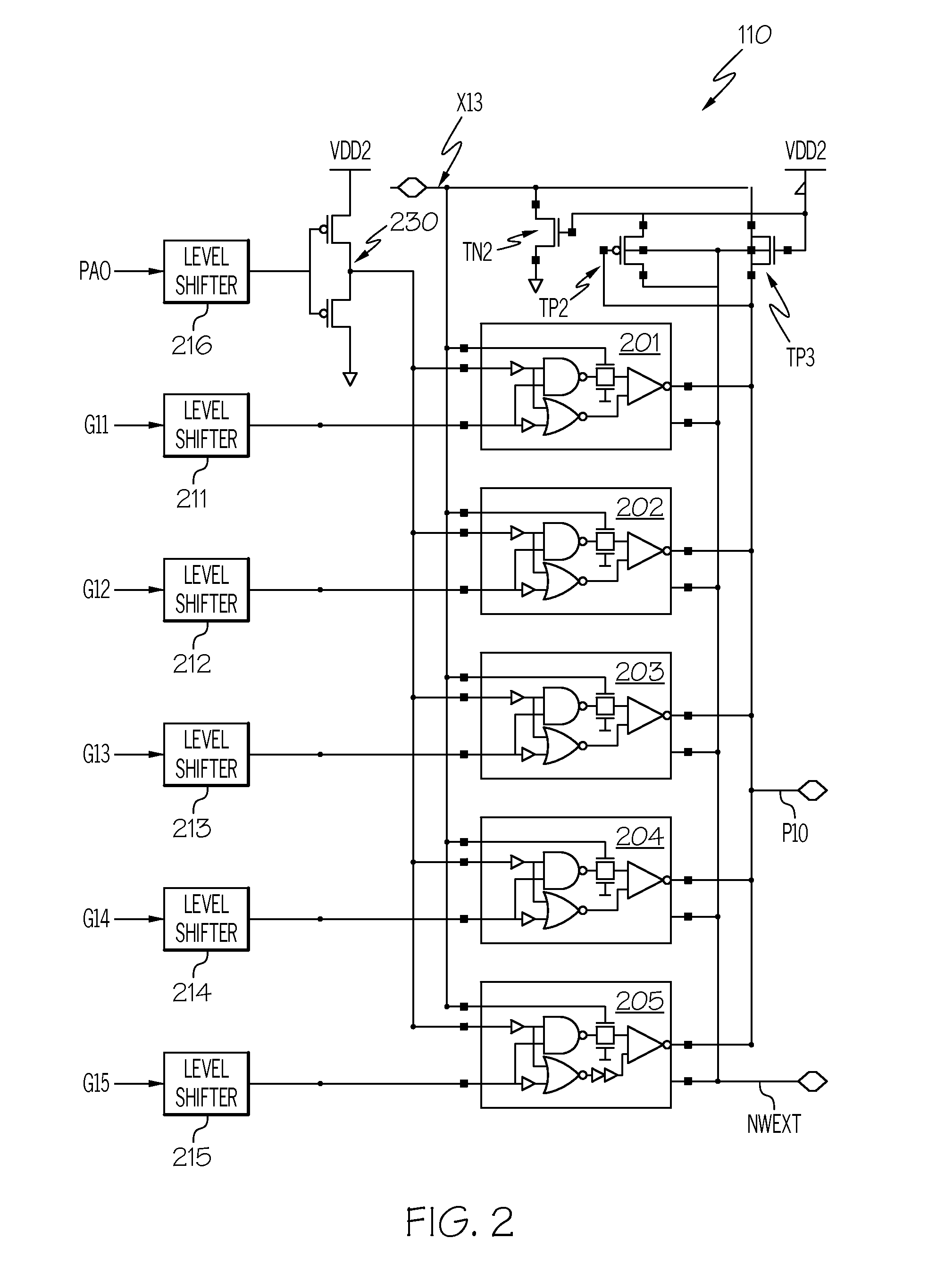
[0018]Referring now to the drawings and in particular to FIG. 1, there is illustrated a block diagram of a programmable transceiver, in accordance with a preferred embodiment of the present invention. As shown, a transceiver 100 includes a driver block 110 and a receiver block 120. Driver block 110 includes a driver input PA0 and programming (control) inputs G11-G15. Similarly, receiver block 120 includes a receiver output P20 and programming (control) inputs REC11-REC14. Both driver block 110 and receiver block 120 share a common input / output (I / O) pin P10. An N-well bias signal, NWext, which is generated by driver block 110, is also connected to receiver block 120. An X13 signal, which is generated by driver block 110, goes to a CMOS switch within both driver block 110 and receiver block 120. This CMOS switch isolates the pre-driver circuits in the driver and receiver functions from the voltage at an external primary I / O pin in cold spare applications.

[0019]With reference now to F...


PUM


Abstract

A multi-function programmable transceiver is described. The transceiver includes a driver circuit and a receiver circuit, which allows an Application Specific Integrated Circuit (ASIC) device to drive and receive data from other ASIC devices. Both the driver and receiver circuits share a common input/output (I/O) pin. The driver circuit can be programmed to provide one of the several driver functions, such as CMOS, TTL, PCI, HSTL, SSTL and LVDS. Other functional features of the transceiver that can be programmed are driving strengths or output impedance, output power supply voltage, single ended or differential mode of HSTL/SSTL transceivers, and class 1 or class 2 operations for SSTL/HSTL transceivers. The receiver circuit can also be programmed to provide one of the several receiver functions, such as CMOS, TTL, PCI, HSTL, SSTL and LVDS.

Description

PRIORITY CLAIM[0001]The present application claims priority under 35 U.S.C. §119(e)(1) to provisional application No. 61 / 522,739, filed on Aug. 12, 2011, the contents of which are incorporated herein by reference.STATEMENT OF GOVERNMENT INTEREST[0002]The present invention was made with United States Government assistance under Contract No. 07-C-0371 awarded by classified customer. The United States Government has certain rights in the present invention.BACKGROUND OF THE INVENTION[0003]1. Technical Field[0004]The present invention relates to receivers and drivers in general, and in particular to a programmable transceiver for Field Programmable Gate Array devices.[0005]2. Description of Related Art[0006]Field Programmable Gate Array (FPGA) devices are commonly employed to implement different functions in various applications. Because of the large numbers of potential applications, FPGA devices will be called upon in various applications to receive input signals from a variety of circ...

Claims


Application Information

Patent Timeline
IPC IPC(8): H03K3/011
CPCH03K3/011H03K19/018585
Inventor BANSAL, JAI P.
Owner BAE SYST INFORMATION & ELECTRONICS SYST INTERGRATION INC
Why Eureka
Try Eureka