Light emitting device with graded composition hole tunneling layer

a technology of composition hole and light emitting device, which is applied in the direction of semiconductor devices, lasers, semiconductor lasers, etc., can solve the problems of affecting the operation of electrons and holes, and affecting the efficiency of light emitting devices

Inactive Publication Date: 2013-09-05
NAT CHIAO TUNG UNIV
View PDF3 Cites 4 Cited by
  • Summary
  • Abstract
  • Description
  • Claims
  • Application Information

AI Technical Summary

Benefits of technology

[0026]Therefore, the advantage and spirit of the present invention can be understood further by the following detail description of invention and attached Figures.

Problems solved by technology

However, due to the internal electric field will be generated upon operating Group III nitride semiconductor devices, the electrons and holes will be hindered by the declined quantum barrier.
It has been mentioned in the prior art that the electron hole distribution of common indium gallium nitride / gallium nitride quantum-well is extremely concentrated in the last quantum-well, which is not advantageous for the operation at high current.
It has also been mentioned in the other prior art that the problem of concentrated electrons and holes can be improved by using thin quantum barrier and changing doping concentration, but the efficacy is quite limited.
The graded quantum barrier height is adopted to change the carrier transport, but only electron overflow is reduced by this way, the problem of electron hole transport still cannot be improved.

Method used


Image

  • Light emitting device with graded composition hole tunneling layer
  • Light emitting device with graded composition hole tunneling layer
  • Light emitting device with graded composition hole tunneling layer

Examples


Embodiment Construction

[0032]The present invention discusses a semiconductor light emitting device. In order to understand the present invention thoroughly, the structure and manufacturing steps of semiconductor light emitting device will be described in detail as follows. Obviously, the implement of the present invention will not limit the special details of semiconductor light emitting device. However, besides describing in detail, the present invention can also be widely implemented in other embodiments, and the range of the invention is not limited, it is subject to the claims and future patent range.

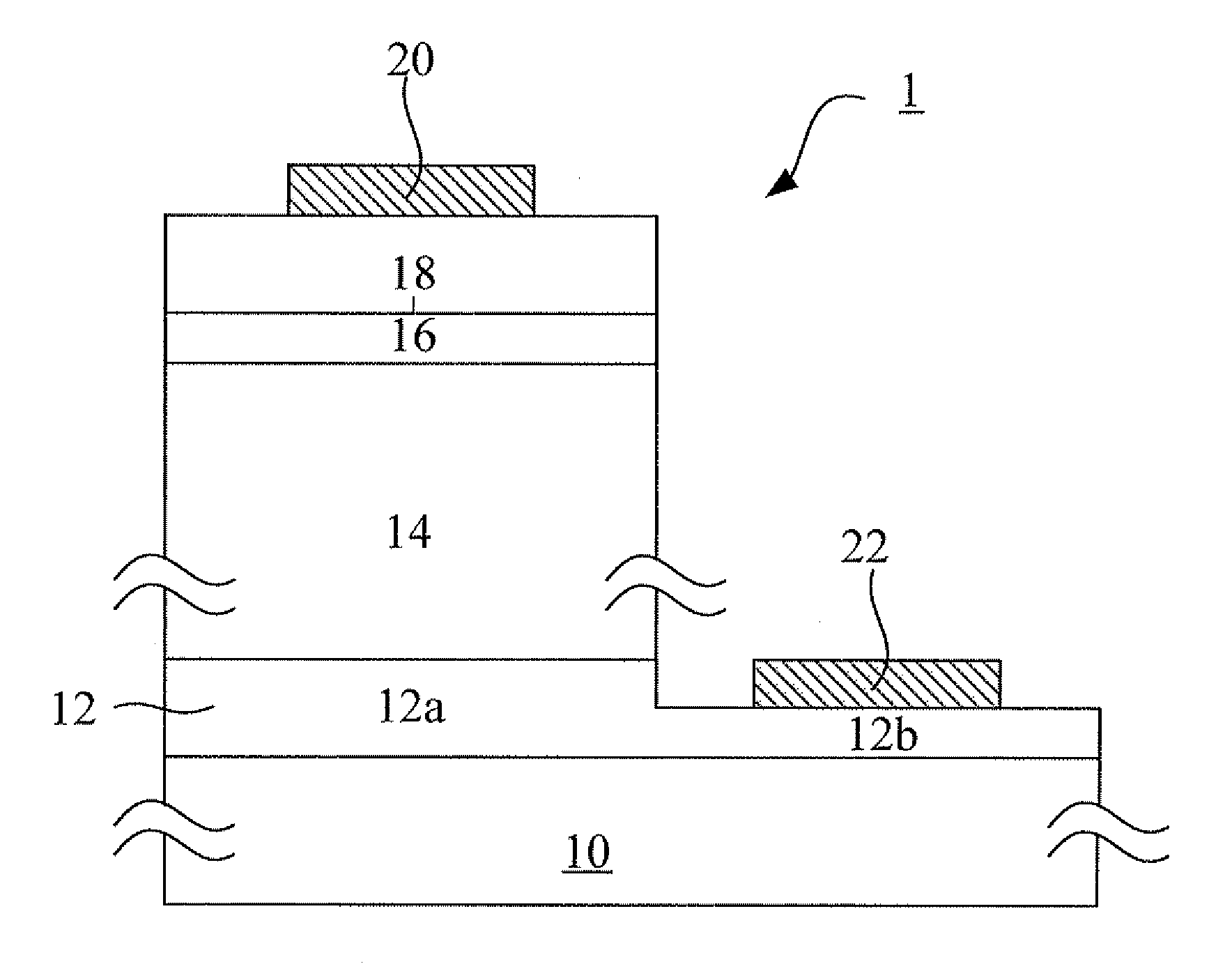
[0033]Please referring to FIG. 1, which is an illustration for an embodiment of a light emitting device with graded composition hole tunneling layer. As shown in FIG. 1, the light emitting device 1 with graded composition hole tunneling layer comprises a substrate 10, an n-type semiconductor layer 12, a graded composition hole tunneling layer 14, an electron blocking layer 16 and a p-type semiconductor la...


PUM


Abstract

A light emitting device with graded composition hole tunneling layer is provided. The device comprises a substrate and an n-type semiconductor layer is disposed on the substrate, in which the n-type semiconductor layer comprises a first portion and a second portion. A graded composition hole tunneling layer is disposed on the first portion of the n-type semiconductor layer. An electron blocking layer is disposed on the graded composition hole tunneling layer. A p-type semiconductor layer is disposed on the electron blocking layer. A first electrode is disposed on the p-type semiconductor layer, and a second electrode is disposed on the second portion of the n-type semiconductor layer and is electrical insulated from the first portion of the n-type semiconductor. The graded composition hole tunneling layer is used as the quantum-well to improve the transport efficiency of the holes to increase the light emitting efficiency of the light emitting device.

Description

BACKGROUND OF THE INVENTION[0001]1. Field of the Invention[0002]The present invention relates a light emitting device, more particularly to a light emitting device with graded composition hole tunneling layer.[0003]2. Description of the Prior Art[0004]In the prior art structure, most wide band gap semiconductor light emitting devices (particularly Group III and Group V nitride) contain the quantum-well as the light emitting layer. The quantum barrier provides the ability for confining the carrier in the light emitting layer. However, due to the internal electric field will be generated upon operating Group III nitride semiconductor devices, the electrons and holes will be hindered by the declined quantum barrier. The transport of electrons and holes in the quantum-well will be blocked, so that the light emitting efficiency will be reduced.[0005]Employing the quantum-well as the light emitting layer has become a very common application of the semiconductor light emitting device, such...

Claims


Application Information

Patent Timeline
Patent Type & Authority Applications(United States)
IPC IPC(8): H01L33/40
CPCH01L33/06H01L33/08H01S5/2009B82Y20/00H01S5/34333H01S5/3416H01S5/3407
Inventor WANG, CHAO-HSUNKUO, HAO-CHUNG
Owner NAT CHIAO TUNG UNIV
Why Eureka
Try Eureka