Semiconductor device having plural standard cells

a technology of semiconductor devices and standard cells, applied in the field of semiconductor devices, can solve the problems of increasing chip size, difficult to fully lay out wiring, and difficulty in miniaturizing power supply wiring in proportion to standard cells, and achieve the effect of reducing the density of the wiring layer lying above the gate wiring layer of a semiconductor device using standard cells

Active Publication Date: 2013-09-05
LONGITUDE LICENSING LTD
View PDF15 Cites 4 Cited by
  • Summary
  • Abstract
  • Description
  • Claims
  • Application Information

AI Technical Summary

Benefits of technology

[0011]According to the present invention, the wiring density of a wiring layer lying above the gate wiring layer of a semiconductor device using standard cells can be reduced.

Problems solved by technology

Even in such cases, power supply wiring can be difficult to miniaturize in proportion to standard cells in order to satisfy characteristic requirements.
However, the wiring may not always be able to be fully laid out.
This increases the chip size.
Such a problem becomes pronounced as the types of power supply potentials needed for the circuit blocks increase.
The reason is that, as mentioned above, the wiring width of power supply wiring is difficult to reduce.

Method used


Image

  • Semiconductor device having plural standard cells
  • Semiconductor device having plural standard cells
  • Semiconductor device having plural standard cells

Examples


second embodiment

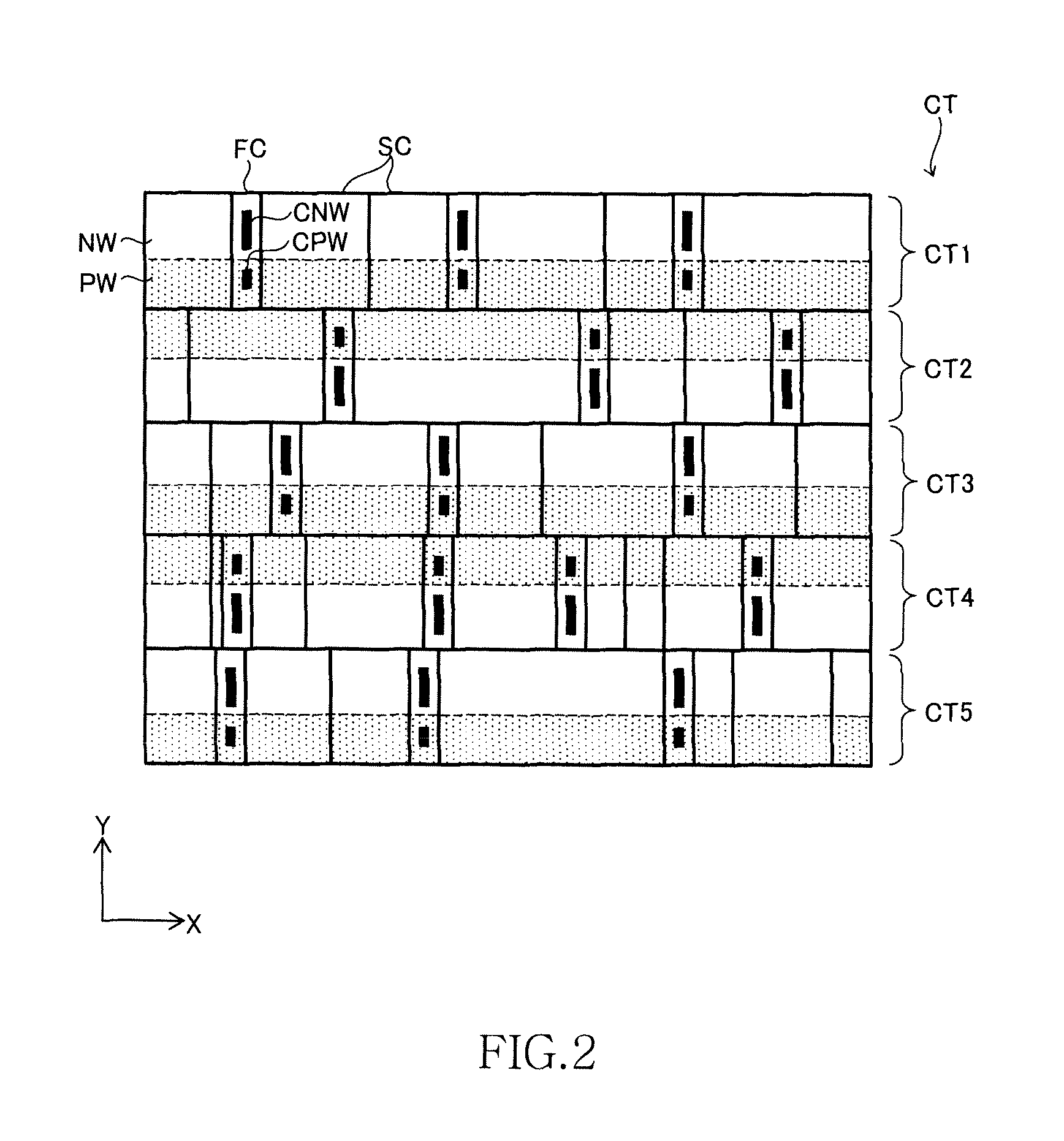
[0082]Turning to FIG. 22, in the present invention, the mesh-like power supply wiring GV formed on the gate wiring layer G is supplied with the low-level power supply potential VSS. Mesh-like power supply wiring M1V formed on the first wiring layer M1 is supplied with the high-level power supply potential VDD. The low-level power supply potential VSS is also used as the well potential of the p-well regions PW. The high-level power supply potential VDD is also used as the well potential of the n-well regions NW. Therefore, the number of the power supply potentials used in the present embodiment is two. The power supply potentials VSS and VDD are supplied from power supply wiring M2S and M2V formed on the second wiring layer M2, respectively.

[0083]The power supply wiring M2S is wiring extending in the X direction. The power supply wiring M2S is connected to a diffusion region DFp formed in the p-well region PW through a contact conductor CPW, and is connected to the mesh-like power su...

first embodiment

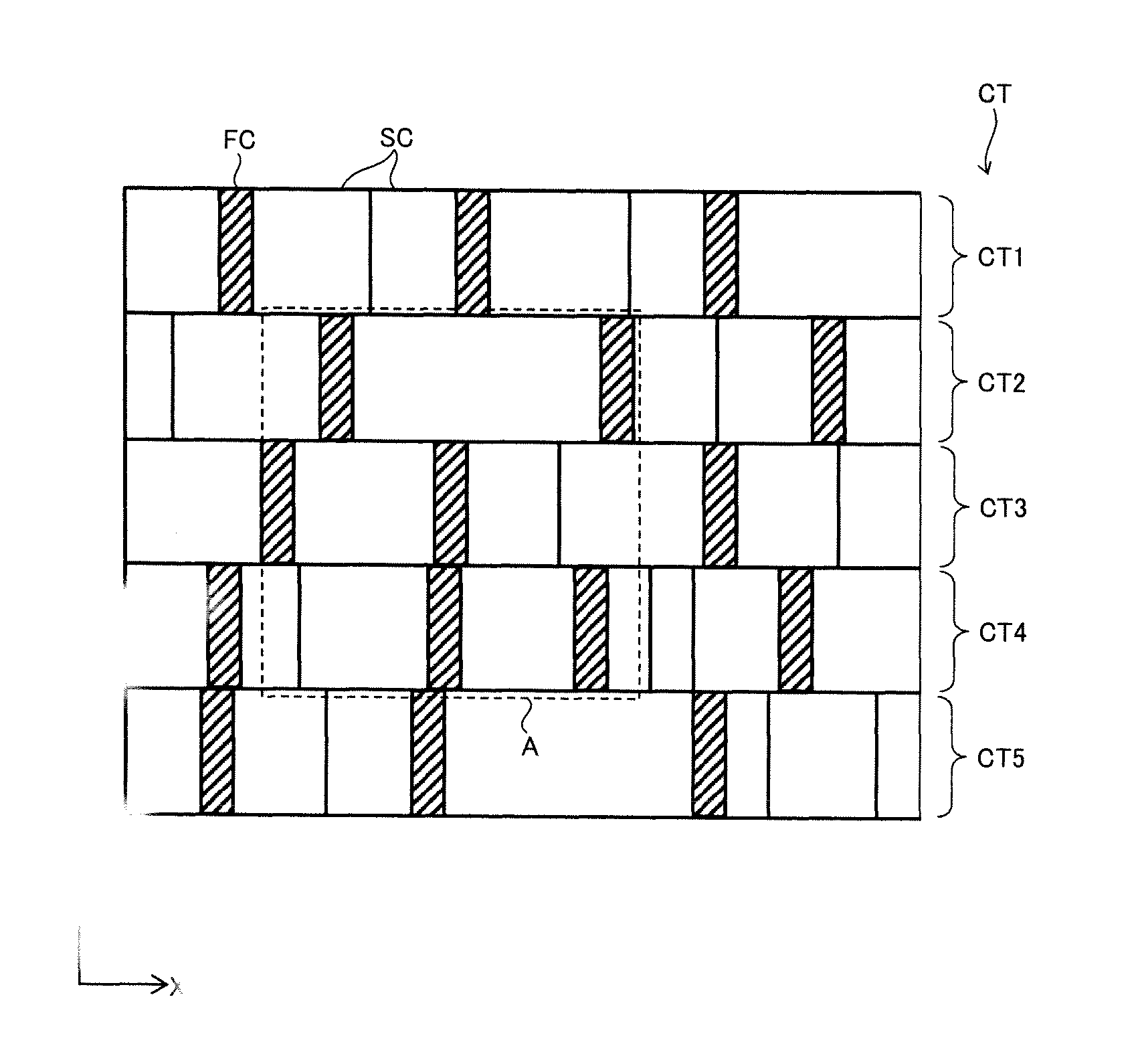
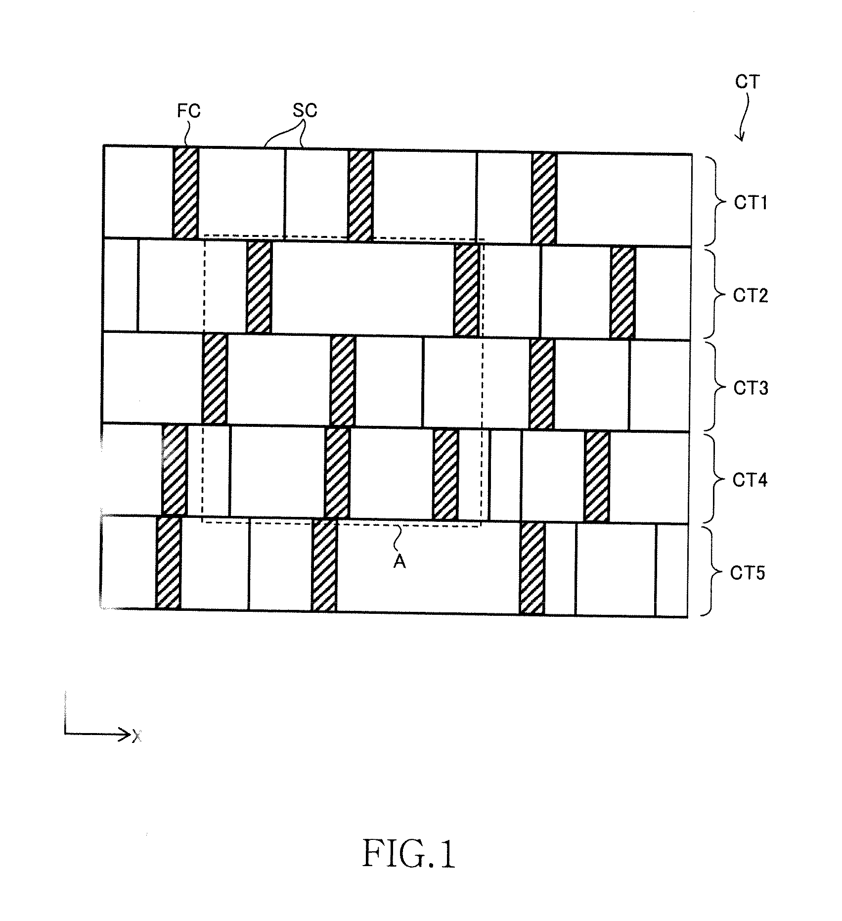
[0085]Even in the example of FIG. 22, the semiconductor device includes a plurality of cell tracks CT. Each cell track CT includes a plurality of standard cells SC and feed cells FC which are arranged in the X direction. In that respect, the present embodiment is the same as the foregoing In the present embodiment, the mesh-like power supply wiring GV is supplied with the power supply potential VSS, and the mesh-like power supply wiring M1V is supplied with the power supply potential VDD. A single power supply wiring M2S and a single power supply wiring M2V can thus be allocated for the plurality of cell tracks CT. This can reduce the wiring density of the wirings formed on the second wiring layer M2.

[0086]In the present embodiment, the power supply wiring GV of the gate wiring layer G forms a mesh of the power supply potential VSS. The gate wiring layer G therefore preferably has a wiring resistance as low as possible. A gate wiring layer G is typically made of doped polysilicon, ...

third embodiment

[0089]Turning to FIG. 23, in the present invention, power supply wiring GVV and GVS formed on the gate wiring layer G extends mainly in the Y direction. Power supply wiring M1V and M1S formed on the first wiring layer M1 extends mainly in the X direction. The power supply wirings GVV and GVS on the gate wiring layer G are arranged in feed cells FC in parallel. The power supply wiring GVV and the power supply wiring M1V are connected via through conductors THv. The power supply wiring GVS and the power supply wiring M1S are connected via through hole conductors THs. Consequently, there are formed two power supply meshes. The power supply potential VDD is supplied to the power supply wiring M1V through a power supply wiring M2V which extends in the X direction on the second wiring layer M2. Similarly, the power supply potential VSS is supplied to the power supply wiring M1S through a power supply wiring M2S which extends in the X direction on the second wiring layer M2.

[0090]The power...


PUM


Abstract

Disclosed herein is a device that includes: a plurality of first standard cells arranged on a semiconductor substrate in a first direction, each of the first standard cells including at least one field-effect transistor; and a first power supply wiring extending in the first direction along one end of the first standard cells in a second direction. The field-effect transistor including a gate electrode formed on a gate wiring layer. The first power supply wiring being formed on the gate wiring layer.

Description

BACKGROUND OF THE INVENTION[0001]1. Field of the Invention[0002]The present invention relates to a semiconductor device, and more particularly to a semiconductor device that includes a circuit block composed of a plurality of standard cells.[0003]2. Description of Related Art[0004]A semiconductor device is typically designed by combining a plurality of needed standard cells to lay out circuit blocks having desired functions on a semiconductor substrate (see Japanese Patent Application Laid-open Nos. 2010-73728, 2000-77609, 2010-129895, and 2008-193070). “Standard cells” refer to pre-registered layouts of logic circuits having basic functions, such as an inverter circuit and a NAND gate circuit. Wirings for establishing internal connections of the standard cells are mainly formed on a first wiring layer that lies above a gate wiring layer. Wiring for connecting the standard cells, wiring for supplying input signals and power supply potentials from outside the circuit blocks, and wiri...

Claims


Application Information

Patent Timeline
Patent Type & Authority Applications(United States)
IPC IPC(8): H01L27/088
CPCH01L27/088H01L27/11807H01L27/0207H01L2027/11881
Inventor SUGIMOTO, SATORUSHIMIZU, TAKANARI
Owner LONGITUDE LICENSING LTD
Why Eureka
Try Eureka