

Semiconductor device
- Summary
- Abstract
- Description
- Claims
- Application Information
AI Technical Summary
Benefits of technology
Problems solved by technology
Method used
Image

Examples
first embodiment
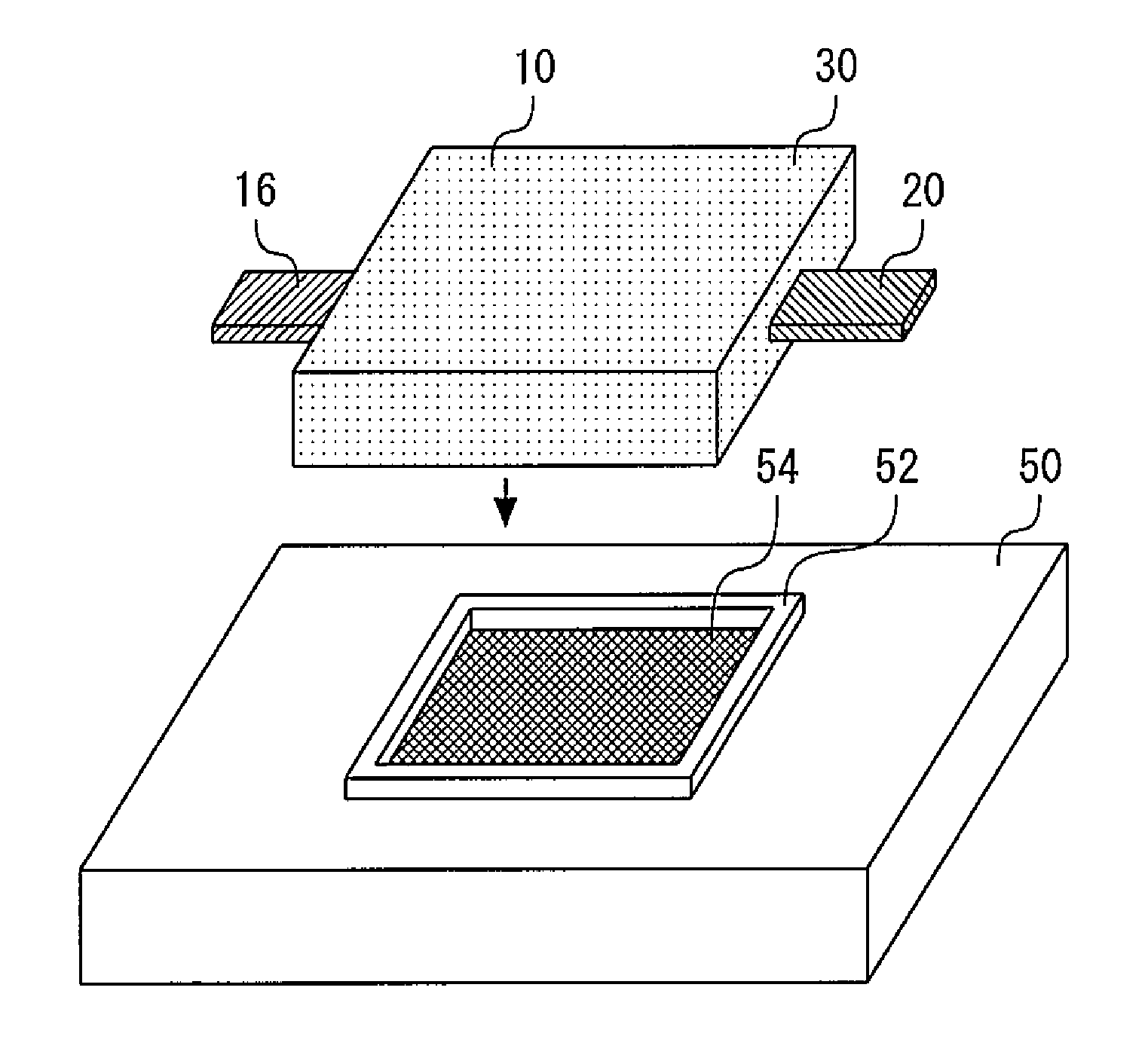
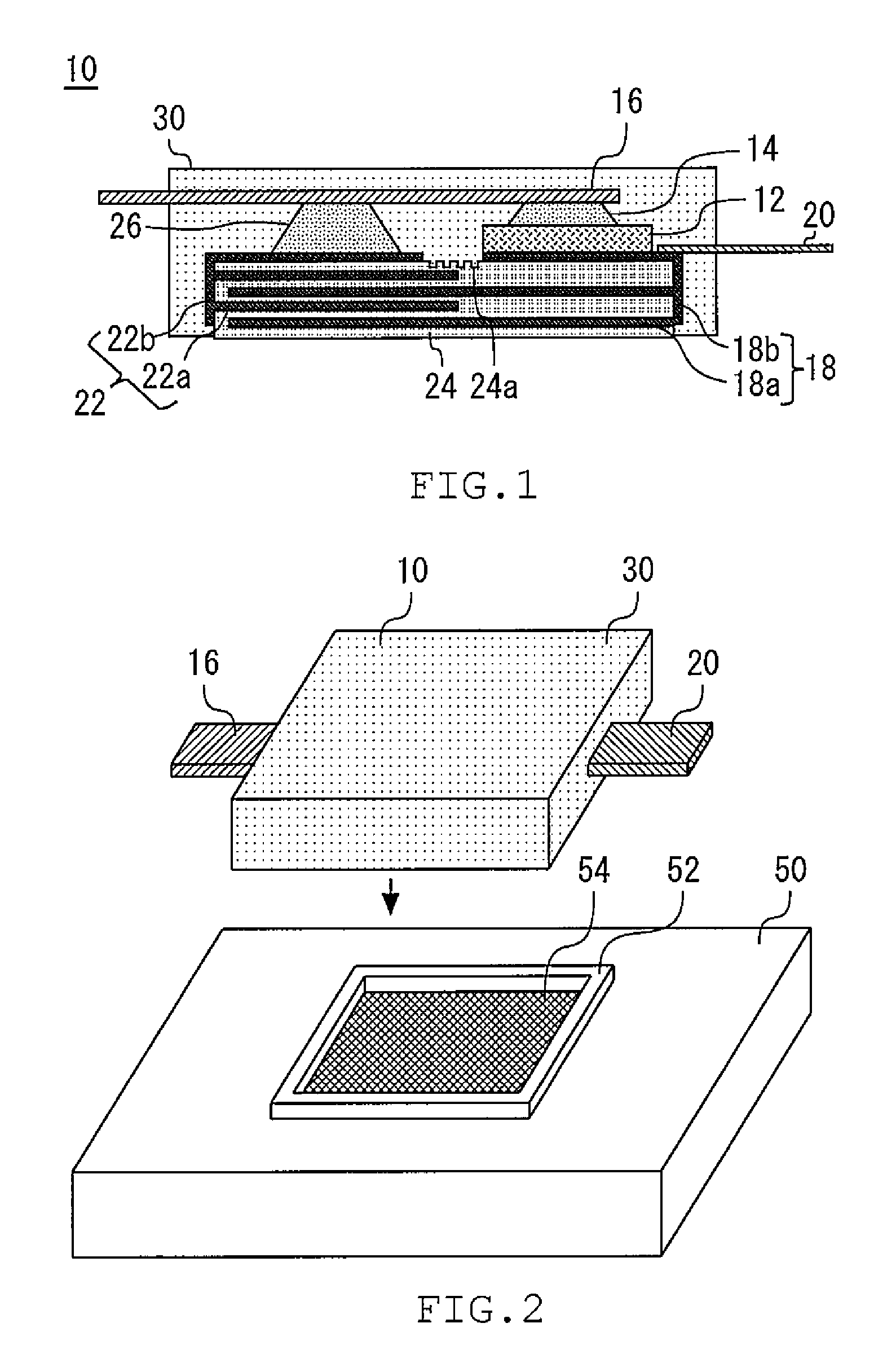
[0018]FIG. 1 is a cross-sectional view of a semiconductor device in accordance with a first embodiment of the present invention. The semiconductor device 10 has a semiconductor element 12. The semiconductor element 12 is an IGBT having an emitter formed on its upper surface and a collector formed on its lower surface. A first electrode 16 is electrically connected to the upper surface of the semiconductor element 12 by solder 14. The first electrode 16 functions as an emitter electrode.
[0019]A first internal electrode 18 is electrically connected to the lower surface of the semiconductor element 12. The first internal electrode 18 has a plurality of first comb finger portions 18a and a first connection portion 18b which connects the first comb finger portions 18a together. The first comb finger portions 18a extend parallel to each other. One of the first comb finger portions 18a is in surface contact with the lower surface of the semiconductor element 12.
[0020]A second electrode 20 ...
second embodiment
[0030]FIG. 5 is a cross-sectional view of a semiconductor device in accordance with a second embodiment of the present invention. The following description of the second embodiment will be primarily limited to the differences from the first embodiment. The semiconductor device of the second embodiment has a third internal electrode 60. The third internal electrode 60 has a plurality of third comb finger portions 60a and a third connection portion 60b which connects the third comb finger portions 60a together. The third internal electrode 60 is electrically connected to the second electrode 20 by solder 62. Specifically, one of the third comb finger portions 60a is connected to the upper surface of the second electrode 20 through the solder 62. It should be noted that the third internal electrode 60 is formed on the upper side of the semiconductor element 12.
[0031]A fourth internal electrode 64 is formed to face the third internal electrode 60. The fourth internal electrode 64 has a ...
third embodiment
[0036]FIG. 6 is a cross-sectional view of a semiconductor device in accordance with a third embodiment of the present invention. The following description of the third embodiment will be primarily limited to the differences from the first embodiment. A first internal electrode 100 and a second internal electrode 102 vertically face each other. Specifically, a first connection portion 100b of the first internal electrode 100 is in surface contact with the lower surface of the semiconductor element 12. Further, a plurality of first comb finger portions 100a extend downward from the first connection portion 100b. The upper surface of a second connection portion 102b of the second internal electrode 102 faces the first connection portion 100b. Further, a plurality of second comb finger portions 102a extend upward from the second connection portion 102b.
[0037]A first electrode 104 is electrically connected to the upper surface of the semiconductor element 12 by solder 14 and is bent int...
PUM
 Abstract
Description
Claims
Application Information