Method for Manufacturing Light-Emitting Device

a technology of light-emitting devices and manufacturing methods, which is applied in the direction of thermoelectric devices, flexible printed circuits, organic semiconductor devices, etc., can solve the problems of burnt deposits, inability to form openings with desired depth, and damage to the bottom or periphery of openings,

Active Publication Date: 2013-09-19
SEMICON ENERGY LAB CO LTD
View PDF7 Cites 79 Cited by
  • Summary
  • Abstract
  • Description
  • Claims
  • Application Information

AI Technical Summary

Benefits of technology

[0019]The method for manufacturing a light-emitting device of one embodiment of the present invention enables light emitted from a light-emitting element to come out from the second organic layer side. Moreover, since light emitted from the light-emitting element can come out through the coloring layer, a desired emission color ...

Problems solved by technology

However, in the case where an opening is formed in the organic film or the substrate by a laser ablation method or the like, the bottom or periphery of the opening might be damaged due...

Method used


Image

  • Method for Manufacturing Light-Emitting Device
  • Method for Manufacturing Light-Emitting Device
  • Method for Manufacturing Light-Emitting Device

Examples


embodiment 1

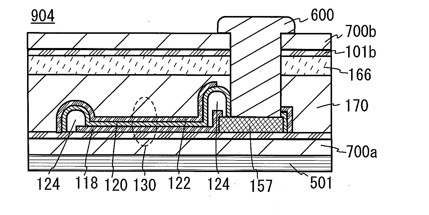
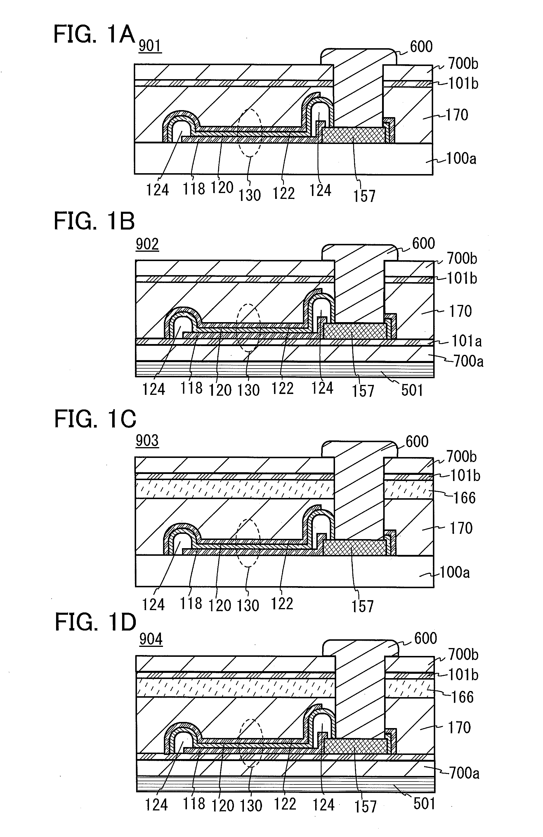
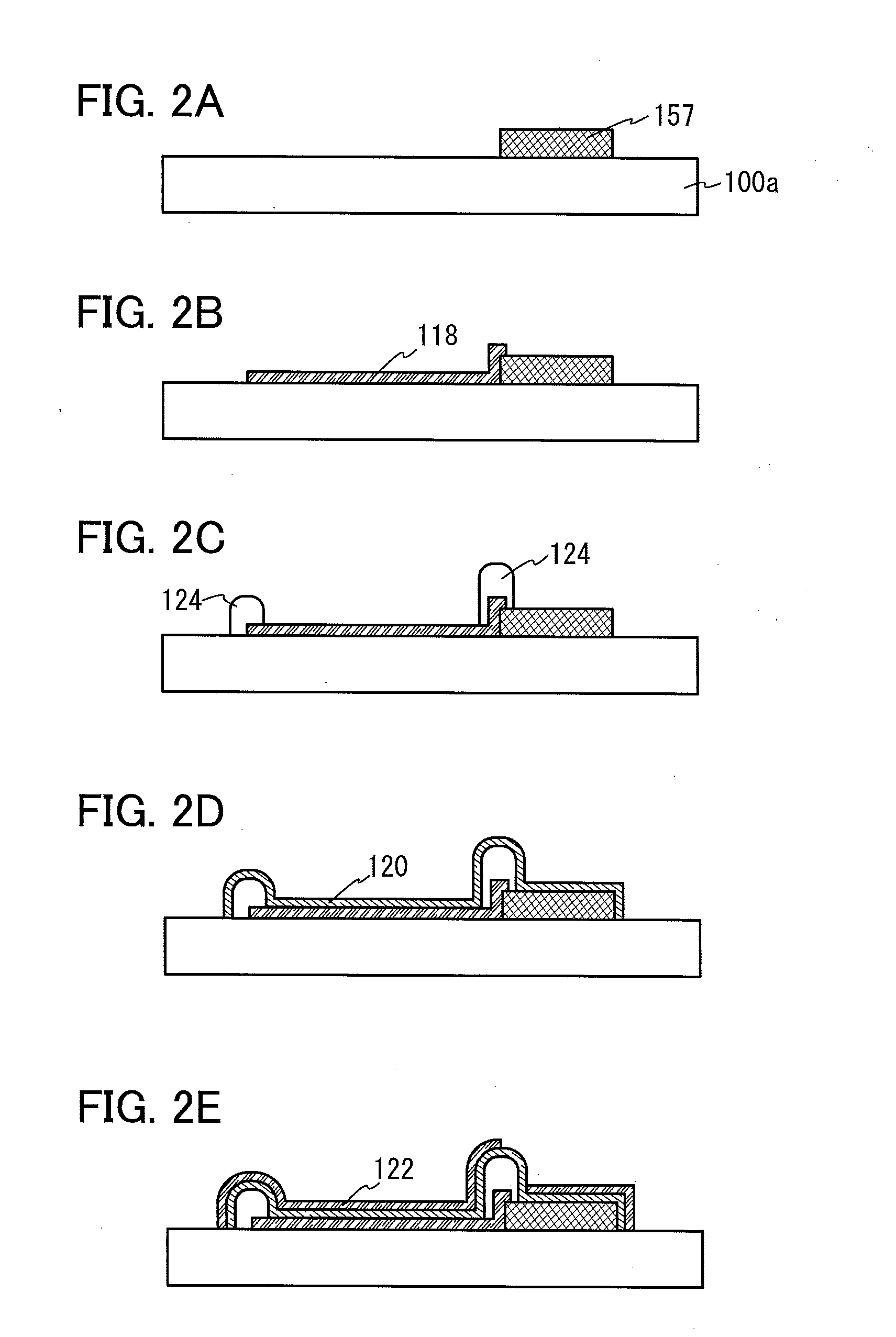
[0038]FIG. 1A is across-sectional view illustrating a light-emitting device 901 which can be manufactured by a method for manufacturing a light-emitting device of one embodiment of the present invention. The light-emitting device 901 includes an electrode terminal 157 and a first electrode layer 118 over a first substrate 100a. An edge portion of the first electrode layer 118 is covered with a partition wall 124 to be insulated. An organic compound-containing layer 120 is in contact with at least the top surfaces of the first electrode layer 118 and the partition wall 124. There is a part in which the organic compound-containing layer 120 does not exist over the electrode terminal 157. A second electrode layer 122 is in contact with at least a top surface of the organic compound-containing layer 120. The second electrode layer 122 does not exist over the electrode terminal 157. An adhesive layer 170 is in contact with the second electrode layer 122. The adhesive layer 170 does not e...

embodiment 2

[0103]In this embodiment, a structure of a light-emitting device of one embodiment of the present invention will be described with reference to FIGS. 7A and 7B, and then a method for manufacturing the light-emitting device will be described with reference to FIGS. 8A to 8D, FIGS. 9A to 9C, FIGS. 10A and 10B, FIGS. 11A and 11B, and FIGS. 12A and 12B.

[0104]FIG. 7A is a top view illustrating a light-emitting device, and FIG. 7B is a cross-sectional view taken along the chain line A1-A2 in FIG. 7A.

[0105]In the light-emitting device illustrated in FIG. 7A, a pixel portion 4502 and a signal line circuit portion 4503 are provided over the flexible substrate 501.

[0106]A transistor 150 which controls the driving of a light-emitting element is provided in each pixel. In FIG. 7B, a transistor 152 which functions as part of the signal line circuit portion 4503 is illustrated.

[0107]The light-emitting device illustrated in FIG. 7B has a structure in which the flexible substrate 501 and a flexible...

embodiment 3

[0192]The light-emitting element 130 illustrated in FIG. 13A has a structure in which the organic compound-containing layer 120 is sandwiched between a pair of electrodes (the first electrode layer 118 and the second electrode layer 122). Note that the first electrode layer 118 is used as an anode and the second electrode layer 122 is used as a cathode as an example in the following description of this embodiment.

[0193]The organic compound-containing layer 120 includes at least a light-emitting layer and may have a stacked-layer structure including a functional layer other than the light-emitting layer. Examples of the functional layer other than the light-emitting layer include a layer containing a substance having a high hole-injection property, a substance having a high hole-transport property, a substance having a high electron-transport property, a substance having a high electron-injection property, and a bipolar substance (a substance having high electron- and hole-transport ...


PUM


Abstract

A method for exposing an electrode terminal covered with an organic film in a light-emitting device without damaging the electrode terminal is provided. In a region of the electrode terminal to which electric power from an external power supply or an external signal is input, an island-shaped organic compound-containing layer is formed and the organic film is formed thereover. The organic film is removed by utilizing low adhesion of an interface between the organic compound-containing layer and the electrode terminal, whereby the electrode terminal can be exposed without damage to the electrode terminal.

Description

BACKGROUND OF THE INVENTION[0001]1. Field of the Invention[0002]The present invention relates to a method for manufacturing a light-emitting device.[0003]2. Description of the Related Art[0004]In recent years, research and development have been extensively conducted on light-emitting elements using electroluminescence (EL). In a basic structure of such a light-emitting element, a layer containing a substance with a light-emitting property is interposed between a pair of electrodes. By voltage application to this element, light emission can be obtained from the light-emitting substance.[0005]The above light-emitting element is a self-luminous element; thus, a light-emitting device using the light-emitting element has advantages such as high visibility, no necessity of a backlight, and low power consumption. The light-emitting device using the light-emitting element also has advantages in that it can be manufactured to be thin and lightweight and has fast response speed.[0006]Since a ...

Claims


Application Information

Patent Timeline
IPC IPC(8): H01L51/56H01L51/52
CPCH01L51/5237H01L51/56H01L27/3246H01L27/1225H01L2227/323H01L2227/326H01L2251/5338H01L27/3276H10K59/122H10K59/131H10K50/844H10K50/8426H10K71/80H10K59/1201H10K71/00H10K2102/311H05K2201/05H10K59/123H10K50/80H10K50/84H10K50/805
Inventor CHIDA, AKIHIROHANATO, KAORUAOYAMA, TOMOYAKOMATSU, RYUKATANIWA, MASATOSHI
Owner SEMICON ENERGY LAB CO LTD
Why Eureka
Try Eureka