Image processing device, imaging device, image processing method, and program

a technology of image processing and imaging device, applied in the direction of picture signal generator, solid-state device signal generator, television system, etc., can solve the problems of s/n degradation and loss of image quality, increase costs, and limit the amount of electrical charge that may be accumulated in the photoelectrical conversion element, etc., to achieve wide dynamic range, poor sn ratio, and wide dynamic range

Active Publication Date: 2013-09-19
SONY SEMICON SOLUTIONS CORP
View PDF3 Cites 43 Cited by
  • Summary
  • Abstract
  • Description
  • Claims
  • Application Information

AI Technical Summary

Benefits of technology

[0050]According to the configuration of an embodiment of the present invention, a device and method are realized to generate an image with a wide dynamic range based on one photographed image. Specifically, an exposure time control is executed to set different exposure times in units of rows of a pixel portion or in units of pixel regions, and multiple, different pixel information, which are pixel values of pixels that have different exposure times set, is obtained. For example, high sensitivity pixel information from long exposure pixels and low sensitivity pixel information from short exposure pixels is obtained, and a pixel value for a

Problems solved by technology

However, there is a limit to the amount of electrical charge that may be accumulated in the photoelectrical conversion elements, and if an amount of light over a certain amount is received, the accumulated electrical charge amount approaches a saturated level, and if a photographic subject region has a brightness that is over a certain amount, a so-called whiteout condition occurs in those regions where a luminosity level has become saturated.
However, for the photographing of photographic subjects with both bright and dark areas, if the shutter is cut at a high speed, the exposure period is not long enough for the dark areas, which results in S/N degradation and loss of image quality.
To perform this proce

Method used


Image

  • Image processing device, imaging device, image processing method, and program
  • Image processing device, imaging device, image processing method, and program
  • Image processing device, imaging device, image processing method, and program

Examples


first embodiment

2-1. First Embodiment

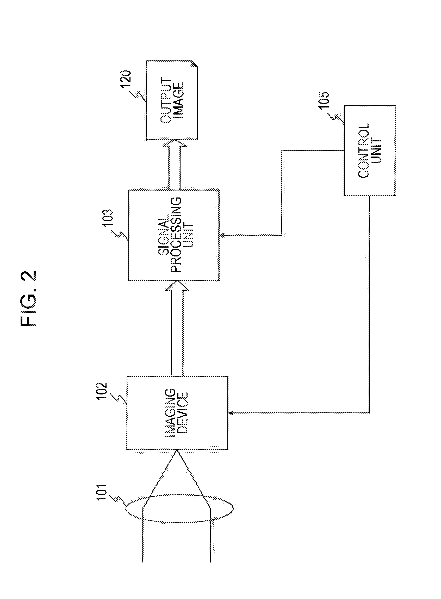
[0079]First, a configuration and processing of the imaging device related to the first Embodiment for the image processing device of the present invention will be described.

[0080]The imaging device 102 of the first Embodiment includes a pixel portion 201 and a calculating unit 202, as illustrated in FIG. 3.

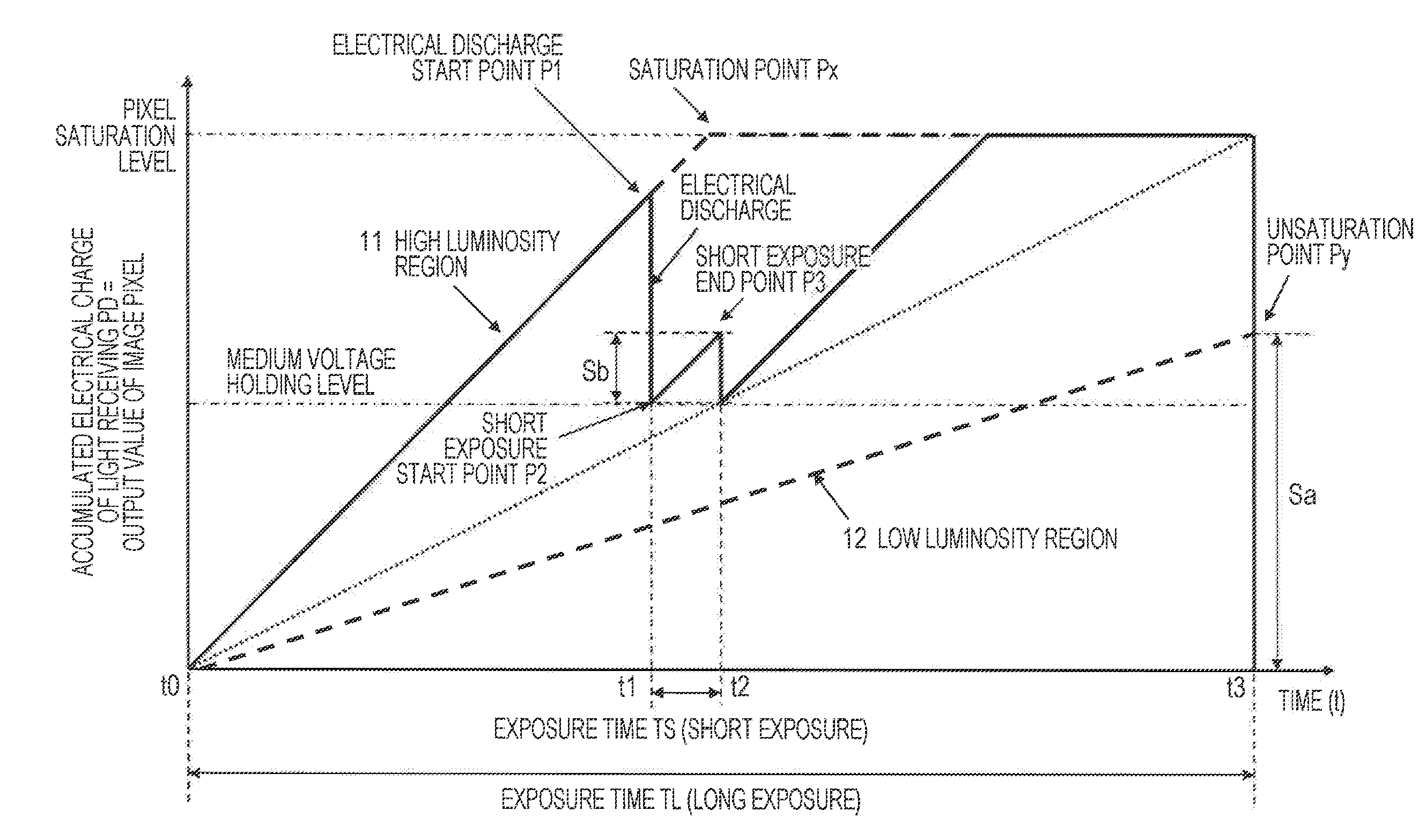
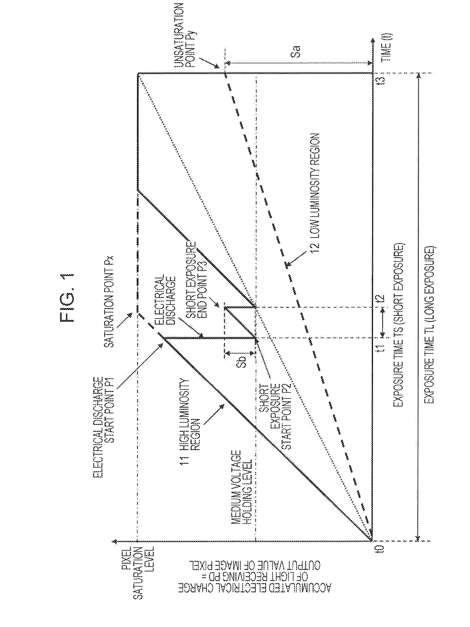
[0081]The pixel portion 201 outputs electrical charge information corresponding to an exposure time by photoelectric conversion of each pixel of a Bayer array pixel array formed with RGB pixels, for example. Regarding the configuration of the first Embodiment, the pixel portion 201 is set with different exposure times in units of pixel regions (rows or lines for example) by control of the control unit 105 (shutter control). A high sensitivity pixel information 251 corresponding to an accumulated electrification based on a long exposure from a row set with a long exposure is output. Also, a low sensitivity pixel information 252 corresponding to an accumulated e...

second embodiment

2-2. Second Embodiment

[0212]Next, as the second Embodiment of the present invention, a configuration and processing examples of an imaging device will be described as having a configuration in which one pixel is selected from the multiple pixels in the AD conversion circuit, and the setting of a pixel value for the output image is performed based on the selected pixel.

[0213]FIG. 11 is a diagram illustrating an example configuration of an imaging device 300 related to the second Embodiment of the present invention. The imaging device 300 includes a pixel portion 301, an output selection unit 302, and a calculating unit 303 as illustrated in the figure. The output selection unit 302 is configured as individual output selection units 302a, 302b, etc. corresponding to the output pixel from each column of the pixel portion 301 as illustrated in FIG. 12, and each output selection unit is configured to include a comparator 321, a counter 322, and a determining unit 323. The calculating uni...

third embodiment

2-3. Third Embodiment

[0254]Next, as the third Embodiment of the present invention, a configuration of a gradation conversion unit after the pixel information combining unit will be described with reference to FIG. 14.

[0255]FIG. 14 is a diagram illustrating a configuration of an imaging device 400 related to the third Embodiment. The configuration illustrated in FIG. 14 has a gradation conversion unit 412 provisioned on the downstream side of the imaging device illustrated in FIG. 3 previously described as the first Embodiment. Other configurations are the same as the configurations for the first Embodiment as illustrated in FIG. 3. Further, the overall configuration of the image processing device (imaging device) is similar to the first Embodiment, and has the configuration previously described with reference toFIG. 2.

[0256]Regarding the imaging device 400 illustrated in FIG. 14, a pixel portion 401 includes a Bayer array of RGbGrB pixels as previously described with reference to FI...


PUM


Abstract

A device and method are provided to generate an image with a wide dynamic range, based on one photographed image. An exposure time control is executed in which different exposure times are set in units of rows of a pixel portion, in units of pixel regions, or similar, and different, multiple pixel information which are the pixel values of the pixels set with different exposures are obtained. For example, high sensitivity pixel information is obtained from long exposure pixels, low sensitivity information is obtained from short exposure pixels, and a pixel value for the output image is calculated based on the pixel information with these different sensitivities. For example, for high luminosity regions, the sensitivity pixel information may have a saturated value, and so a large weight is set to the low sensitivity pixel information, also for low luminosity regions, the SN ratio of low sensitivity pixel information is estimated to be poor, and so a large weight is set to the high sensitivity pixel information to determine the output pixel value.

Description

TECHNICAL FIELD[0001]The present invention relates to an image processing device, an imaging device, an image processing method, and a program. It particularly relates to an image processing device, an imaging device, an image processing method, and a program which generates images with a wide dynamic range.BACKGROUND ART[0002]Solid-state imaging elements, such as CCD image sensors and CMOS (Complementary Metal Oxide Semiconductor) image sensors used in video cameras, digital still cameras, and such, accumulate electrical charges corresponding to an amount of incident light, and perform photoelectric conversion to output electrical signals corresponding to the accumulated electrical charge. However, there is a limit to the amount of electrical charge that may be accumulated in the photoelectrical conversion elements, and if an amount of light over a certain amount is received, the accumulated electrical charge amount approaches a saturated level, and if a photographic subject region...

Claims


Application Information

Patent Timeline
IPC IPC(8): H04N5/235
CPCH04N5/2353H04N5/2351H04N5/3458H04N2209/045H04N5/35554H04N5/35581H04N9/045H04N5/3535H04N23/71H04N25/533H04N25/583H04N25/589H04N23/10H04N25/447H04N23/843H04N25/133H04N25/135H04N25/134H04N23/73
Inventor KASAI, MASANORI
Owner SONY SEMICON SOLUTIONS CORP
Why Eureka
Try Eureka