

Vibration device and method for manufacturing vibration device
- Summary
- Abstract
- Description
- Claims
- Application Information
AI Technical Summary
Benefits of technology
Problems solved by technology
Method used
Image

Examples
Embodiment Construction
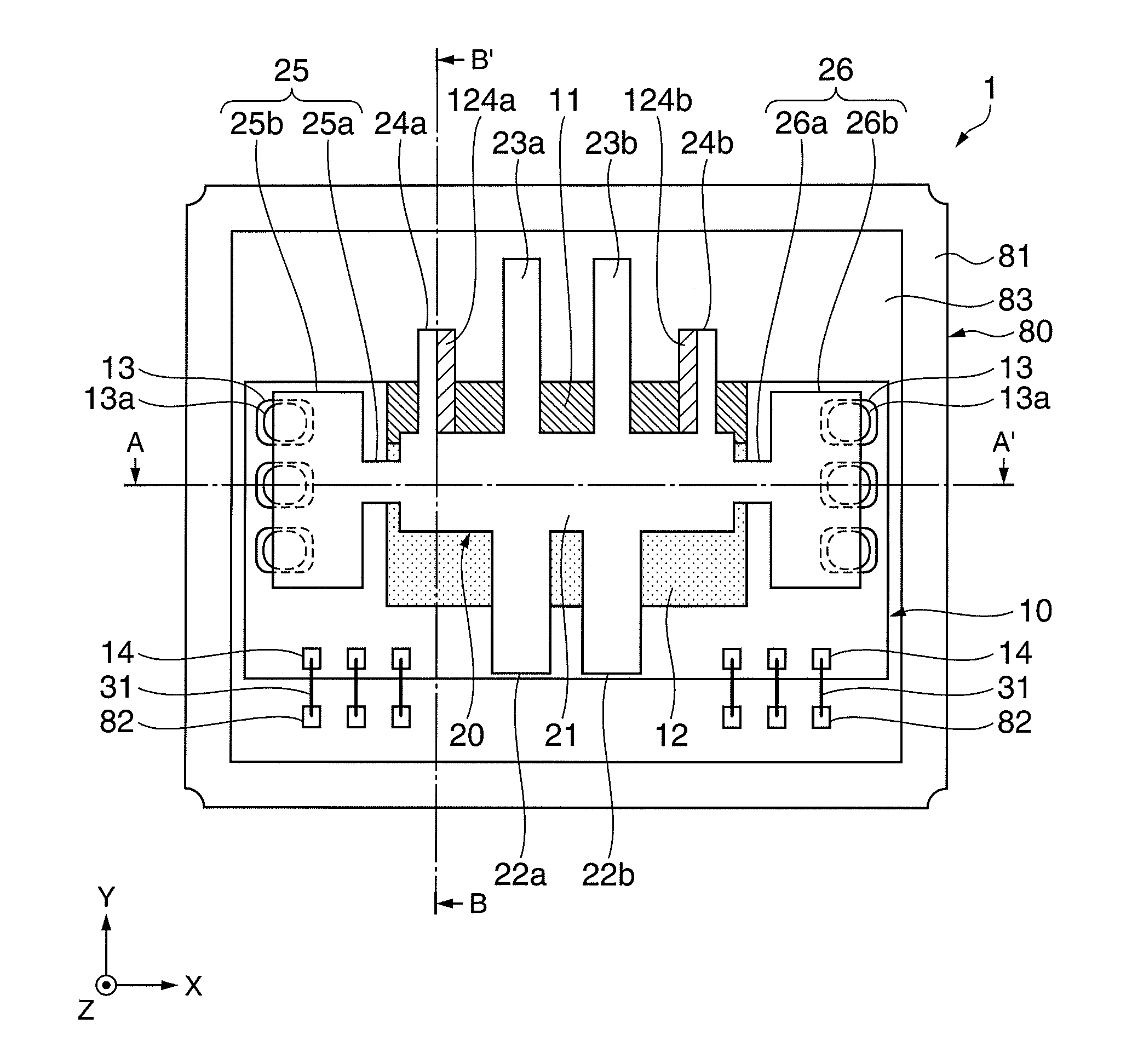
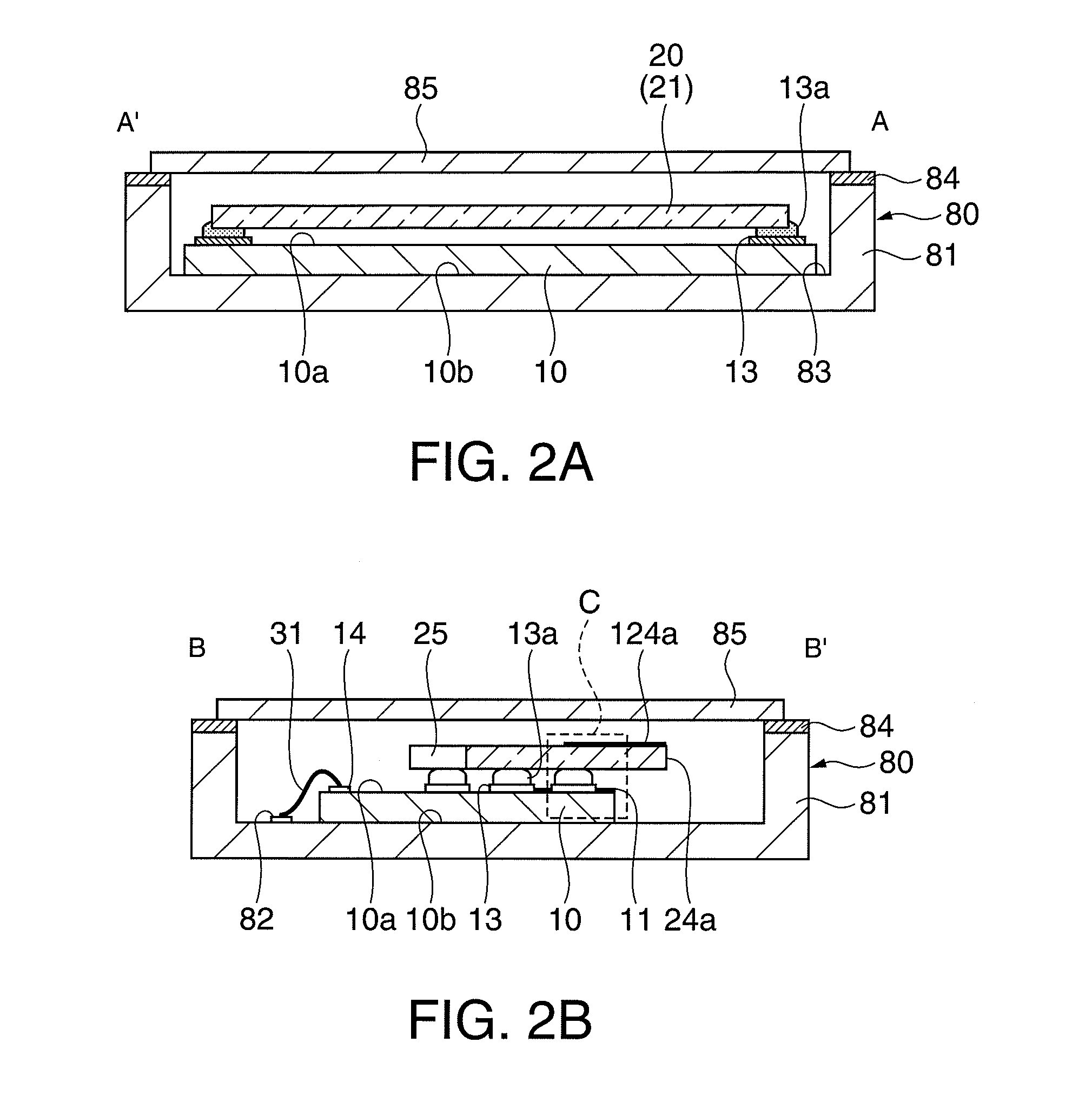
[0023]An embodiment of the invention will be described with reference to the accompanying drawings. In each of the drawings, the size and the ratio of each component may be illustrated different from those of an actual component as needed, so that each of the components assumes the size to the extent that they can be recognized on the drawings. Moreover, an XYZ orthogonal coordinate system is set in each of the drawings, and the relative position of each component will be described referring to the XYZ orthogonal coordinate system. A predetermined direction in a vertical plane is assumed to be an X-axis direction, a direction orthogonal to the X axis direction in the vertical plane is assumed to be a Y-axis direction, and a direction perpendicular to both of the X-axis direction and the Y-axis direction is assumed to be a Z-axis direction. Also, when the direction of gravity is set as reference, the direction of gravity is assumed to be a downward direction and its opposite directio...
PUM
| Property | Measurement | Unit |
|---|---|---|
| Thickness | aaaaa | aaaaa |
| Mass | aaaaa | aaaaa |
Abstract
Description
Claims
Application Information