Light emitting apparatus and its driving method

a technology driving method, which is applied in the direction of electroluminescent light source, electric lighting source, and use of semiconductor lamps, etc., can solve the problems of increasing the number of components, deteriorating contrast, and difficult microminiaturization of light emitting apparatus

Inactive Publication Date: 2013-10-03
CANON KK
View PDF7 Cites 3 Cited by
  • Summary
  • Abstract
  • Description
  • Claims
  • Application Information

AI Technical Summary

Benefits of technology

[0007]It is an aspect of the invention to provide a microminiaturized light emitting apparatus which can prevent a light emission of an EL that is caused by unnecessary electric charges accumulated in a parasitic capacitor and a driving method of the light emitting apparatus.

Problems solved by technology

However, when the source or drain of the driving transistor has a parasitic capacitor, if electric charges charged in the parasitic capacitor flow into the EL, a current which is not concerned with the gradation data flows into the EL and a light emission occurs, so that the contrast deteriorates.
However, according to Japanese Patent Application Laid-Open No. 2010-262251, since a transistor which connects a dedicated reference voltage line and the driving circuit and a controlling wiring of such a transistor are necessary in order to pull out the unnecessary electric charges, and a microminiaturization of the light emitting apparatus is difficult due to an increase in number of component parts.
Therefore, the technique disclosed in Japanese Patent Application Laid-Open No. 2010-262251 is not suitable in the case where the microminiaturization of the light emitting apparatus is required.

Method used


Image

  • Light emitting apparatus and its driving method
  • Light emitting apparatus and its driving method
  • Light emitting apparatus and its driving method

Examples


embodiment 1

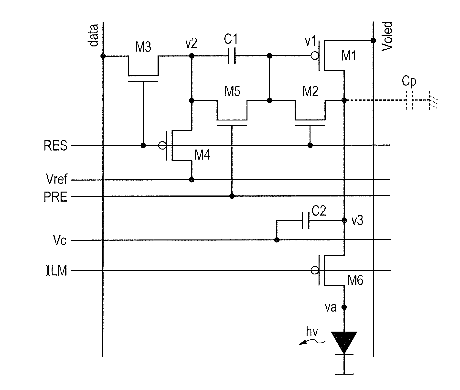
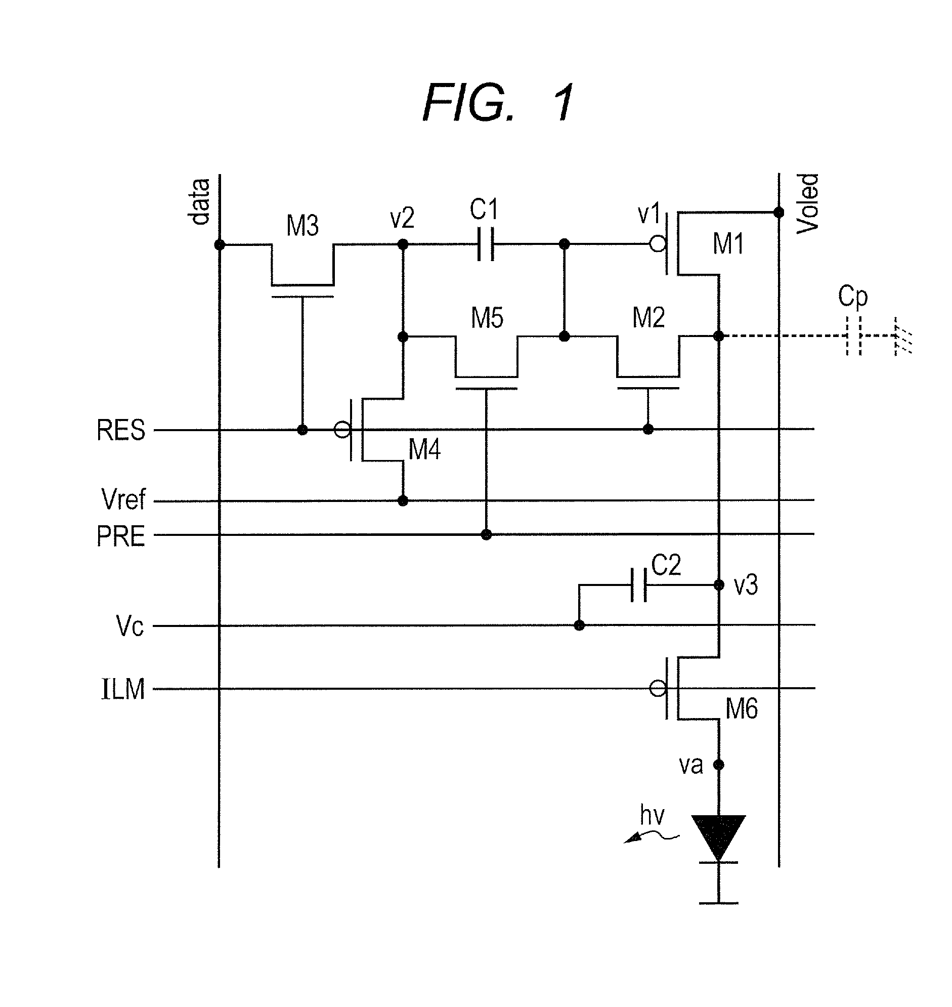
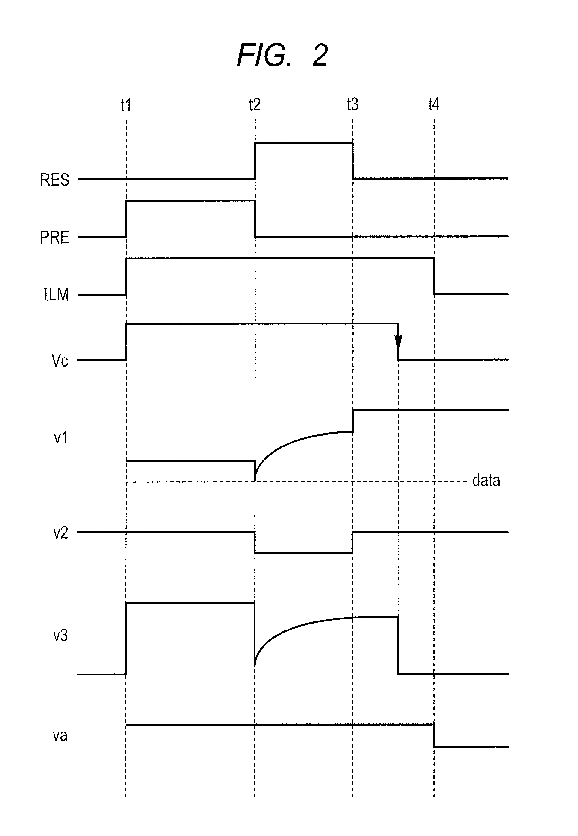
[0052]In the embodiment, the apparatus is driven by using a driving circuit in FIG. 4 in accordance with a timing chart of FIG. 5.

[0053]The driving circuit in FIG. 4 differs from the driving circuit in FIG. 1 with respect to a point that the scanning signal ILM is supplied in place of supplying the control signal Vc. Since there is no need to provide a wiring of the control signal line for supplying the control signal Vc, it is desirable in terms of a point that the light emitting element can be microminiaturized.

[0054]At time t4, the scanning signal ILM changes from H to L. In order to set the drain voltage (v3) of the driving transistor to a value which is equal to or lower than the threshold voltage for initiating the light emission of the EL, the capacitance value of the capacitor C2 is set to a value which satisfies the following condition when assuming that the amplitude of the scanning signal ILM is equal to ΔVilm.

C2≧Cp / [{ΔVilm / (Voled−Vth−ELVth)}−1]

[0055]A forming method of t...

embodiment 2

[0064]In this embodiment, the apparatus is driven by using a driving circuit in FIG. 8 in accordance with a timing chart of FIG. 9.

[0065]The driving circuit in FIG. 8 differs from the driving circuit in FIG. 1 with respect to a point that the scanning signal RES is supplied in place of supplying the control signal Vc. Since there is no need to provide a wiring of the control signal line for supplying the control signal Vc, it is desirable in terms of a point that the light emitting element can be microminiaturized.

[0066]At time t3, the scanning signal RES changes from H to L. In order to set the drain voltage (v3) of the driving transistor to a value which is equal to or lower than the threshold voltage for initiating the light emission of the EL, the capacitance value of the capacitor C2 is set to a value which satisfies the following condition when assuming that the amplitude of the scanning signal RES is equal to ΔVres.

C2≧Cp / [{ΔVres / (Voled−Vth−ELVth)}−1]

[0067]As a forming method ...


PUM


Abstract

A light emitting apparatus wherein, after setting a voltage of a light emitting luminance into a gate of the driving transistor, until setting a light emission controlling transistor at an electrically conducting state, a control signal changing toward a voltage of an opposite electrode of the light emitting element is supplied to the other terminal of the capacitor constructed such that an electro-conductive layer supplied with the control signal and a semiconductor layer forming the terminal of the driving transistor at the side of the light emitting element, a semiconductor layer forming a terminal of a transistor different from the driving transistor and connected to the terminal of the driving transistor at the side of the light emitting element, or an electro-conductive layer connected to the terminal of the driving transistor at the side of the light emitting element are formed so as to face through an insulating layer.

Description

BACKGROUND OF THE INVENTION[0001]1. Field of the Invention[0002]The present invention relates to a light emitting apparatus having a light emitting element and a driving method of the light emitting apparatus and, more particularly, to a light emitting apparatus for controlling a light emission of an organic electroluminescence (EL) element as a current controlling element and a driving method of the light emitting apparatus.[0003]2. Description of the Related Art[0004]As a driving circuit for driving an organic EL (hereinbelow, simply referred to as “EL”), there is a driving circuit having such a construction that a data voltage according to gradation data is supplied to a gate of a driving transistor and a current according to the data voltage is supplied to the EL connected to a source or a drain of the driving transistor. According to the light emitting apparatus using the EL as a light emitting element of such a driving circuit, a black luminance can be set to zero in principle...

Claims


Application Information

Patent Timeline
Patent Type & Authority Applications(United States)
IPC IPC(8): H05B33/08H05B44/00
CPCH05B33/0824H05B33/08H05B45/44H05B45/00Y02B20/30H05B44/00
Inventor IKEDA, KOUJI
Owner CANON KK
Why Eureka
Try Eureka