Shared terminal of an image sensor system for transferring image data and control signals

a technology of image data and control signals, applied in the field of imaging systems, can solve the problems of limiting the overall size of image sensors, limiting the size of endoscopes so as to access various small spaces inside the body, and becoming ever more difficult to accommodate the number of bonding pads

Active Publication Date: 2013-10-10
OMNIVISION TECH INC
View PDF5 Cites 85 Cited by
  • Summary
  • Abstract
  • Description
  • Claims
  • Application Information

AI Technical Summary

Problems solved by technology

For example, the need for the endoscopes to be smaller so as to access various small spaces inside the body may be limited by the size of the image sensors mounted on the endoscopes.
This is due to the size and pitch requirements o...

Method used


Image

  • Shared terminal of an image sensor system for transferring image data and control signals
  • Shared terminal of an image sensor system for transferring image data and control signals
  • Shared terminal of an image sensor system for transferring image data and control signals

Examples


Embodiment Construction

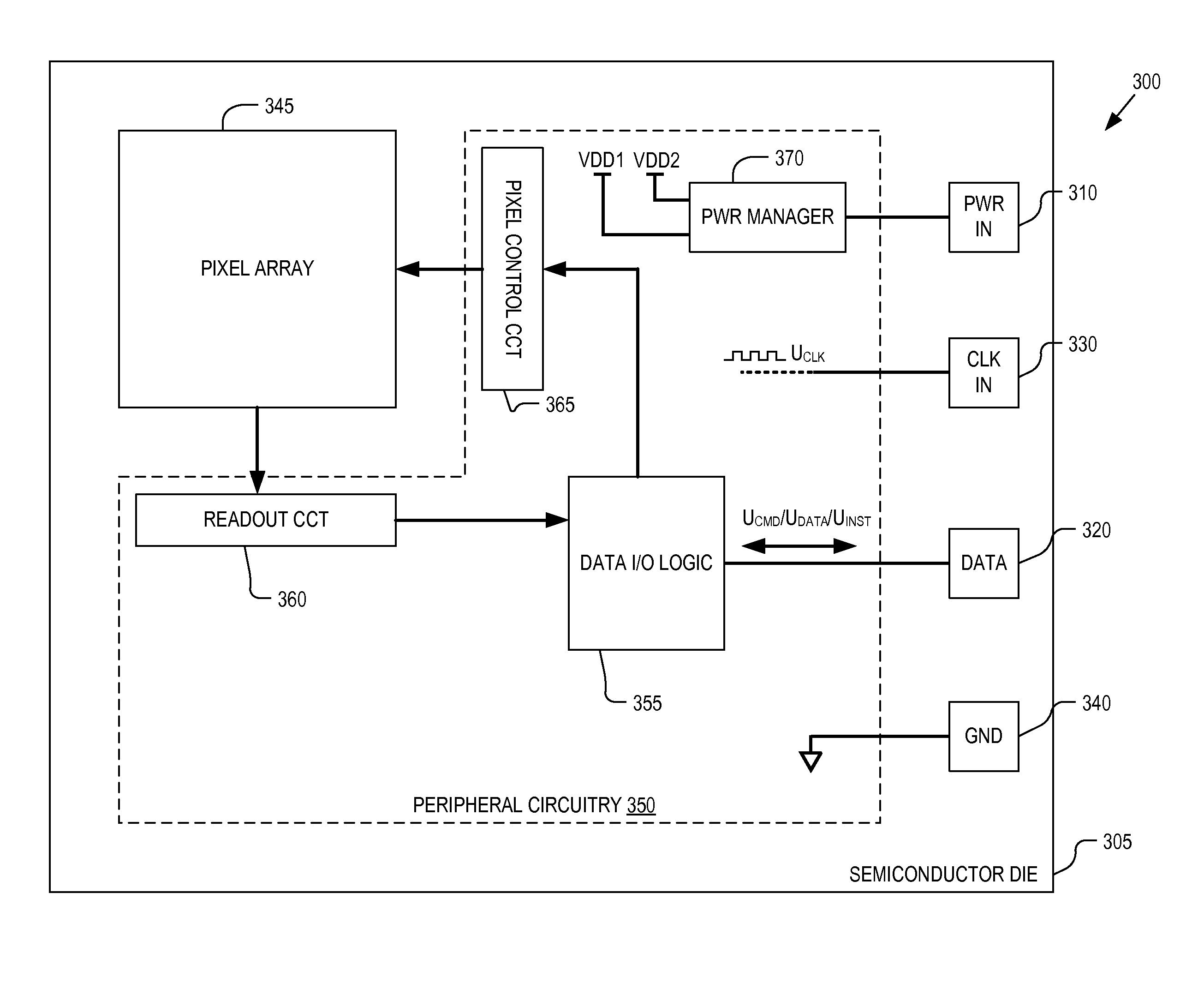
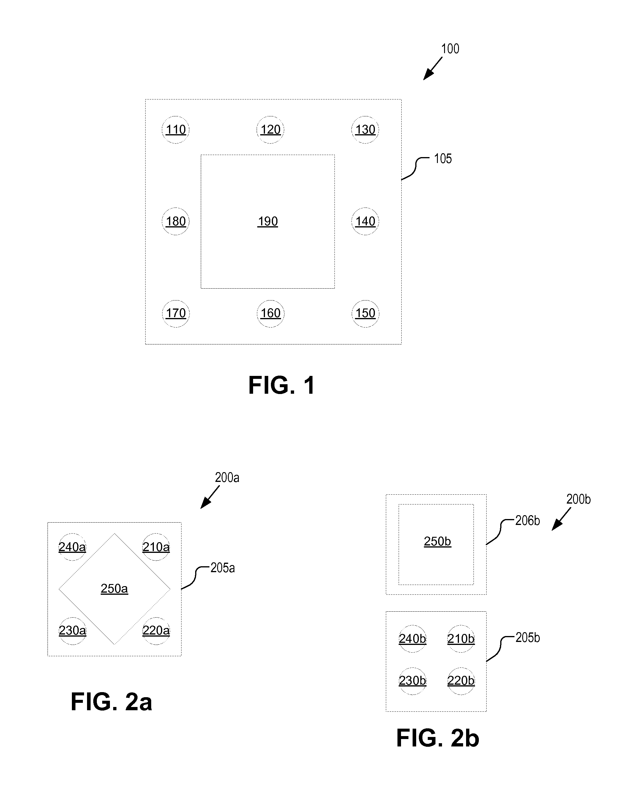
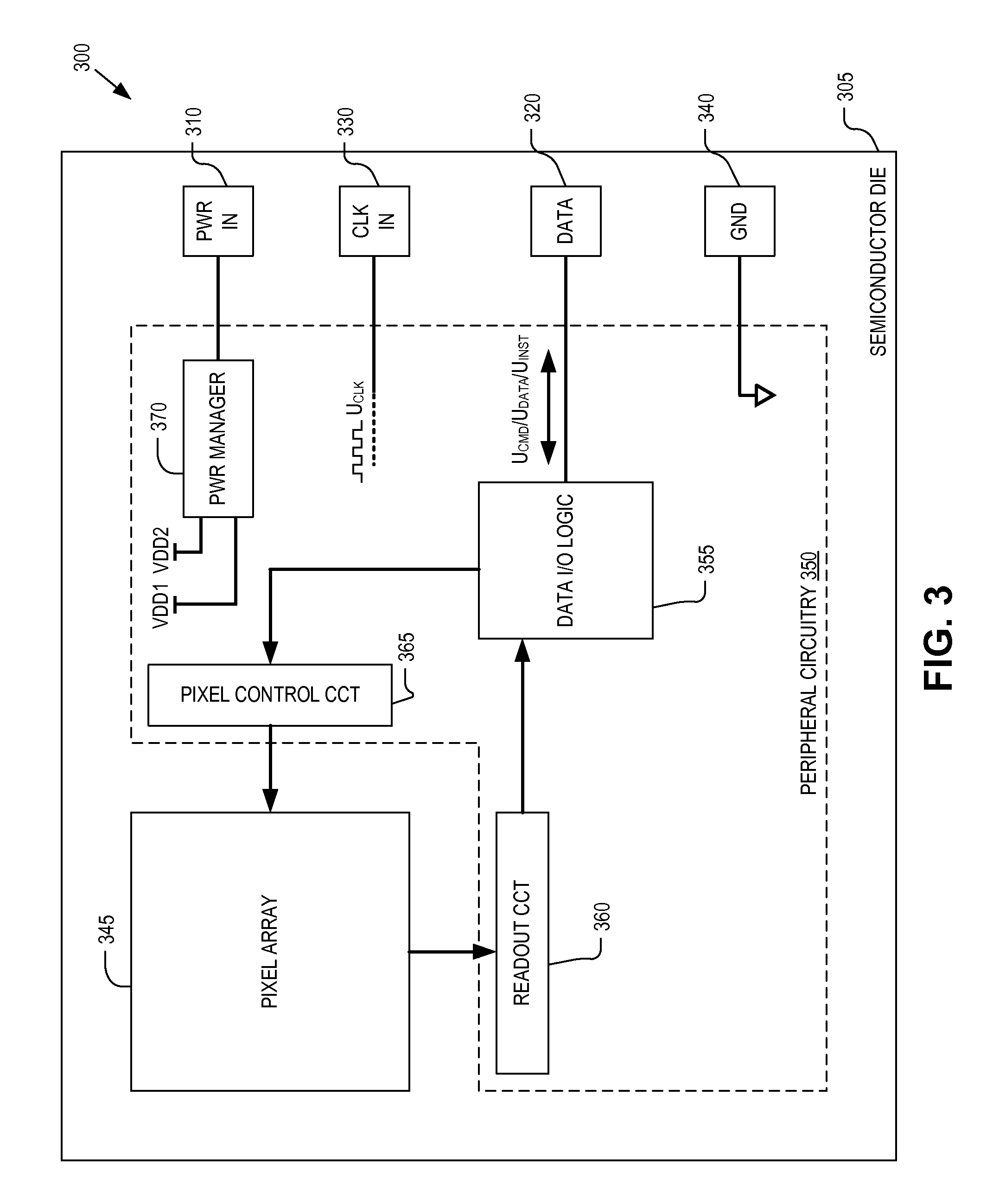
[0017]In the following description numerous specific details are set forth to provide a thorough understanding of the embodiments. One skilled in the relevant art will recognize, however, that the techniques described herein can be practiced without one or more of the specific details, or with other methods, components, materials, etc. In other instances, well-known structures, materials, or operations are not shown or described in detail to avoid obscuring certain aspects.

[0018]Reference throughout this specification to “one embodiment” or “an embodiment” means that a particular feature, structure, or characteristic described in connection with the embodiment is included in at least one embodiment of the present invention. Thus, the appearances of the phrases “in one embodiment” or “in an embodiment” in various places throughout this specification are not necessarily all referring to the same embodiment. Furthermore, the particular features, structures, or characteristics may be co...


PUM


Abstract

An example image sensor system includes an image sensor having a first terminal and a host controller coupled to the first terminal. Logic is included in the image sensor system, that when executed transfers analog image data from the image sensor to the host controller through the first terminal of the image sensor and also transfers one or more digital control signals between the image sensor and the host controller through the same first terminal.

Description

TECHNICAL FIELD[0001]This disclosure relates generally to imaging systems, and in particular but not exclusively, relates to imaging systems having a sensor and a controller.BACKGROUND INFORMATION[0002]Image sensors are widely used in digital cameras, cellular phones, security cameras, as well as, medical, automobile, and other applications. One type of image sensor is known as a complementary metal-oxide-semiconductor (CMOS) image sensor. Multiple CMOS image sensors are typically formed on a semiconductor wafer that is then separated into several dies, each die including at least one image sensor. The semiconductor die is then assembled into a semiconductor package. The semiconductor package provides protection and includes pins, leads, or other chip-scale interfaces, which are then used to connect with circuits that are external to the package. The semiconductor die may be formed having a plurality of bonding pads on the surface of the die for internally connecting (e.g., wire bon...

Claims


Application Information

Patent Timeline
IPC IPC(8): H01L27/146
CPCH01L27/14601H04N5/335H04N5/23241H04N5/378H04N5/369H04N23/65H04N25/00H04N25/70H04N25/75
Inventor DAI, TIEJUNLEI, JUNZHAO
Owner OMNIVISION TECH INC
Why Eureka
Try Eureka