

Touch panel
- Summary
- Abstract
- Description
- Claims
- Application Information
AI Technical Summary
Benefits of technology
Problems solved by technology
Method used
Image

Examples
first embodiment
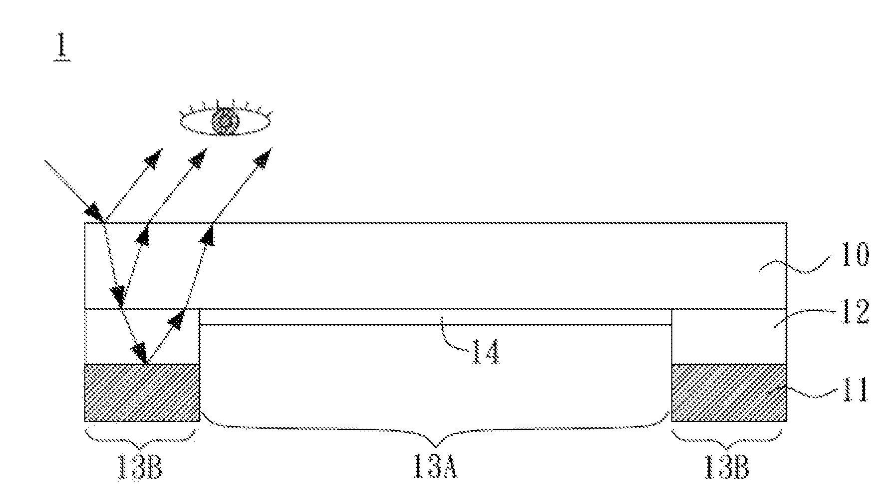
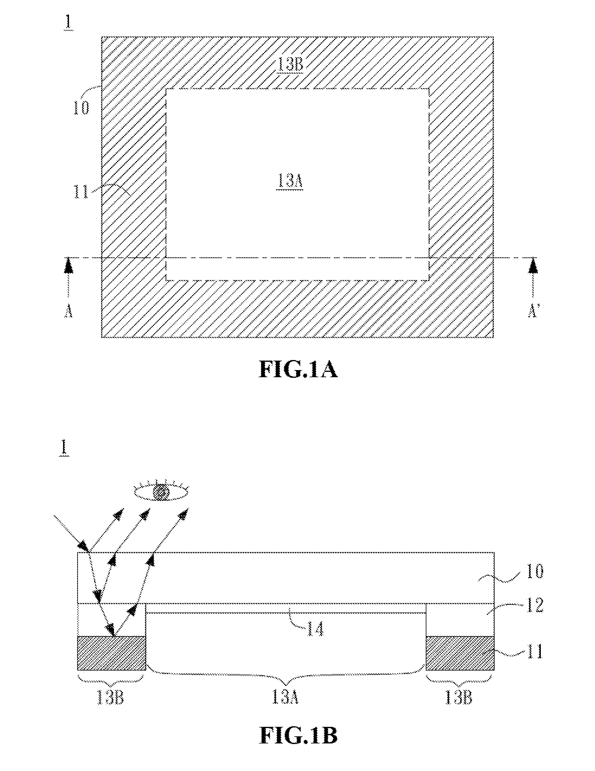
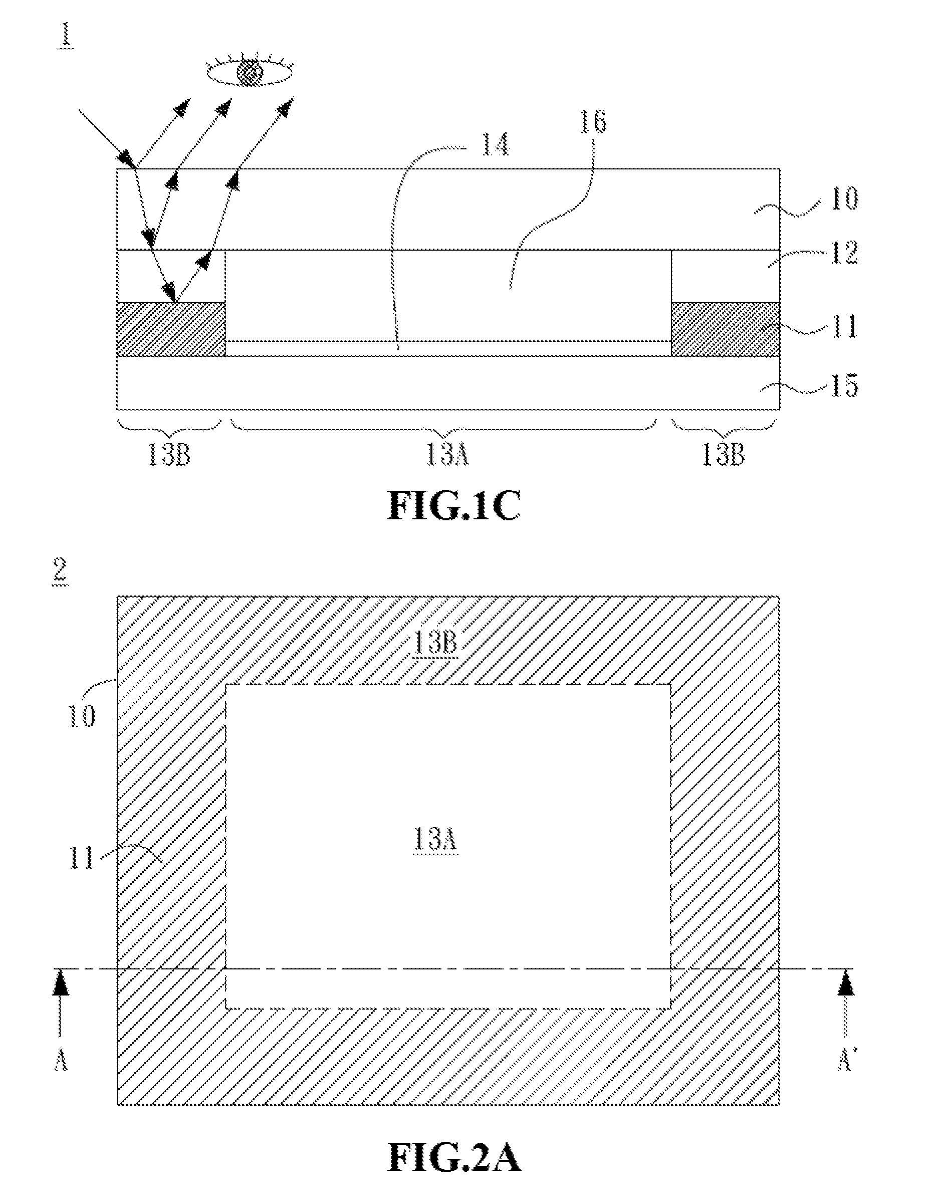
[0015]FIG. 1A and FIG. 1B illustrate a touch panel in accordance with the present disclosure, wherein FIG. 1A is a top view and FIG. 1B is a sectional view, both of which only show important components to emphasize characteristics of the present disclosure. As shown in the FIGS. 1A and 1B, important components of a touch panel 1 include a plate 10, a border 11, a sensing layer 14, and an optical compensation layer 12. The plate 10 has an upper surface and a lower surface opposite to the upper surface and corresponding to users, wherein a sensing region 13A and a conducting wire region 13B are planned on the lower surface. The conducting wire region 13B surrounds the sensing region 13A. In other embodiments, the conducting wire region 13B can also be distributed on any two corresponding sides (not shown) of the sensing region 13A. The border 11 is overlaid on the conducting wire region 13B, and the sensing layer 14 is disposed in the sensing region13A. An optical compensation layer 1...
second embodiment
[0021]FIG. 2A and FIG. 2B illustrate a touch panel 2 in accordance with the present disclosure, wherein FIG. 2A is a top view and FIG. 2B is a sectional view. As shown in the FIGS. 2A and 2B, the touch panel 2 and the touch panel 1 of FIG. 1 have same components and the only difference is that the optical compensation layer 12 of the touch panel 1 of FIG. 1B is disposed on the edge of the plate 10, and placed substantially corresponding to position of the border 11, while an optical compensation layer 12 of the touch panel 2 of FIG. 2B is substantially disposed on the entire surface of a plate 10, and a sensing layer 14 is formed on the lower surface of the optical compensation layer 12 to correspond to position of a sensing region 13A.
[0022]The sensing layer 14 is normally formed by patterning a transparent conductive material (such as ITO or the like), and includes a region covered with the conductive material and a region not covered with the conductive material, wherein refracti...
third embodiment
[0024]FIG. 3A illustrates a touch panel in accordance with the present disclosure. In this embodiment, an optical compensation layer 12 includes one or a plurality of refractive index layers. Although this embodiment has been explained using the structure of FIG. 1A / B, the proposed structure can also be applied in the embodiment of FIG. 2A / B. In this embodiment, the optical compensation layer 12 includes a first refractive index layer 12A and a second refractive index layer 12B, wherein refractive index of the first refractive index layer 12A is less than that of the second refractive index layer 12B. As shown in FIG. 3B, in another embodiment, positions of the first refractive index layer 12A and the second refractive index layer 12B are swapped.
[0025]In another embodiment, sensing layer 14 is not formed plate 10 as shown in FIG. 3C. Although the structure of FIG. 3C is based on the structure of FIG. 3A, the sensing layer 14 of FIG. 3C can also be applied on the structure of FIG. 3...
PUM
 Abstract
Description
Claims
Application Information