

Plasma display panel and manufacturing method of the same
- Summary
- Abstract
- Description
- Claims
- Application Information
AI Technical Summary
Benefits of technology
Problems solved by technology
Method used
Image

Examples
first embodiment
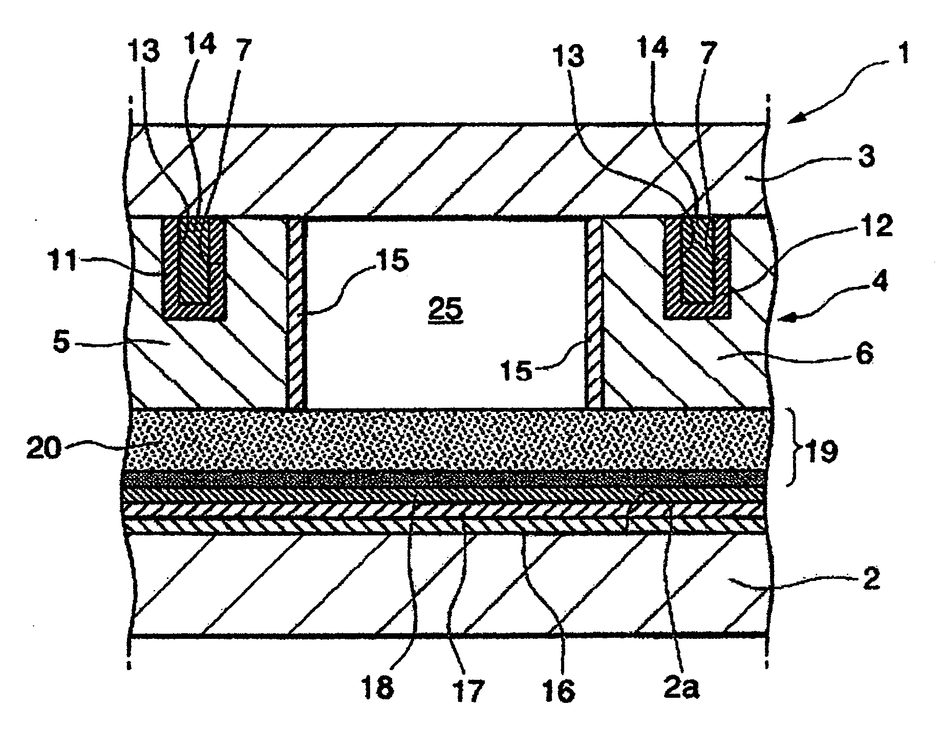
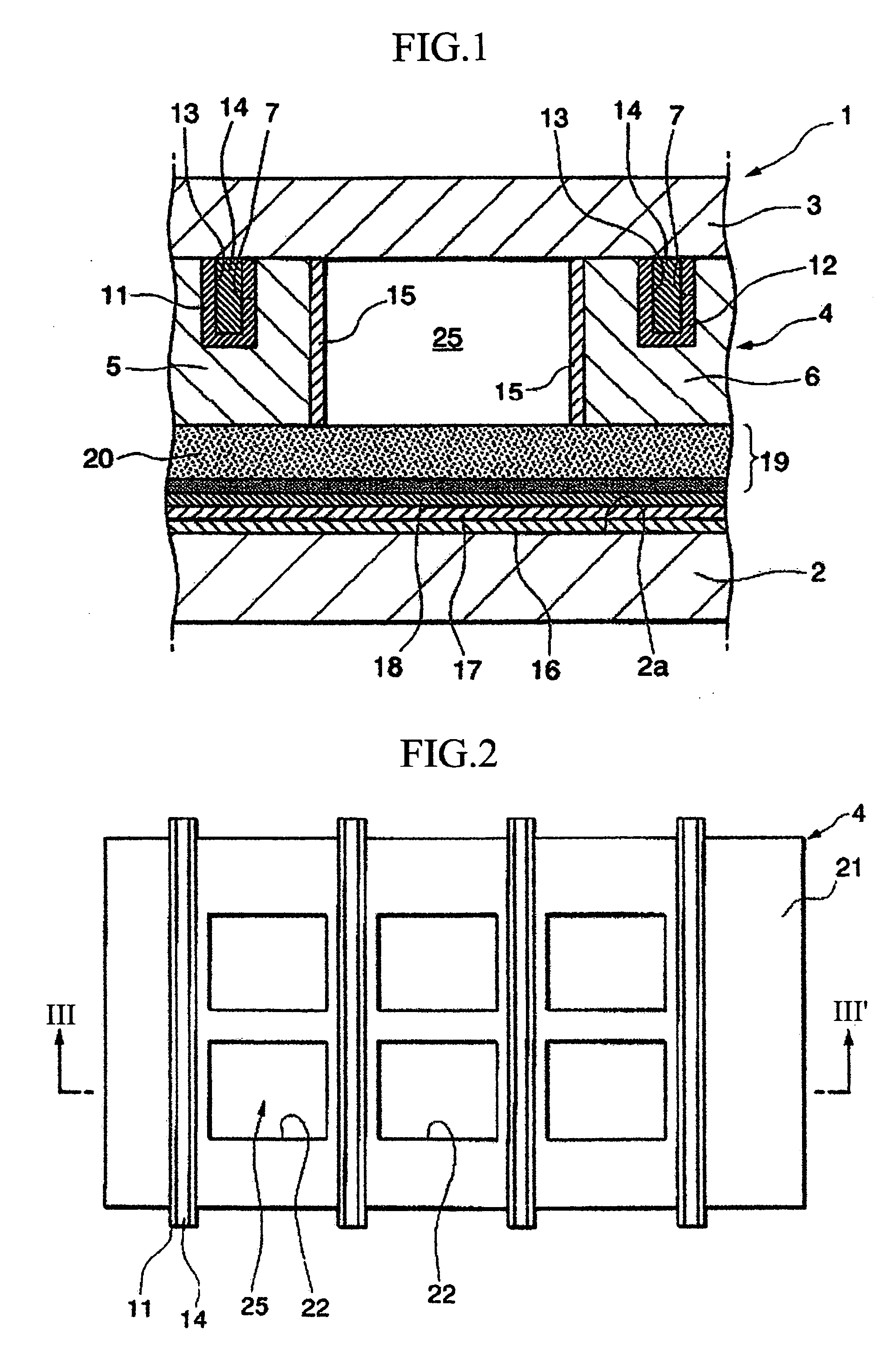
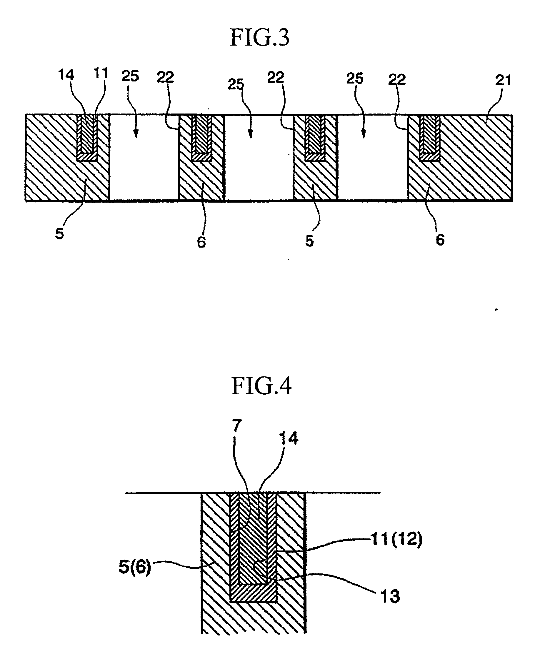
[0033] Referring to FIG. 1 through FIG. 4, the plasma display panel 1 includes a front substrate 3 and a rear substrate 2 facing each other. The front substrate 3 and the rear substrate 2 may be formed of a transparent material such as glass. A barrier rib layer 4 made of a dielectric substance is formed between the front substrate 3 and the rear substrate 2. Discharge spaces 25 are formed in the barrier rib layer 4 corresponding to each of discharge cells, and a discharge gas is filled into the discharge spaces 25. The radiation of light is generated by plasma discharge, thereby displaying an image on the front substrate 3. The barrier rib layer 4 includes barrier rib members 5 and 6, grooves 7 formed in the barrier rib members 5 and 6, and display electrodes 11 and 12 formed on the inner surface of the grooves 7. The barrier rib members 5 and 6 are formed in a matrix pattern, defining a plurality of discharge cells. The grooves 7 are formed to extend in a predetermined direction ...
third embodiment
[0079]FIG. 10 and FIG. 11 are process views showing the manufacturing method of a PDP 201 according to the present invention.
[0080] Firstly, a dielectric layer 133, which is a base material of a barrier rib layer 204, is formed on a front substrate 3 (FIG. 10A). The dielectric layer 133 is formed in the same way as in the first and second embodiments.
[0081] Subsequently, a resist 134 for sandblasting is laminated on the dielectric layer 133 using a laminator (FIG. 10B), and a mask layer M5 for patterning the resist 134 is arranged over the resist 134. In this mask layer M5, first openings M6 corresponding to the display electrodes and second openings M7 corresponding to the discharge spaces are formed. The first openings M6 may be formed in a predetermined pattern, for example, in a stripe or a matrix pattern. In addition, the second openings M7 may be formed in a predetermined pattern, for example, in a stripe or a matrix pattern.
[0082] The resist 134 for sandblasting is then exp...
second embodiment
[0091] The undercoating layer 16 through the phosphor layer 20 and the lower barrier rib members 105a and 106a are successively formed on the inner surface 2a of the rear substrate 2. The front substrate 3 having the barrier rib layer 204 and the rear substrate 2 are then aligned and attached to each other such that the discharge spaces 225a formed on the front substrate 3 and the discharge spaces 125b formed on the rear substrate 2 are integrated (FIG. 11B). Thereafter, the periphery of the attached PDP 201 is sealed with a sealing material such as glass frit, and a discharge gas such as Xe gas is injected into the integrated discharge spaces 225, thereby completing the manufacture of the PDP 201 according to the present embodiment (FIG. 11C). Thus, the construction of the PDP according to the present embodiment is substantially the same as the construction of the
[0092] According to the manufacturing method of the PDP 201 of the present embodiment, the discharge spaces 225a and the...
PUM
 Abstract
Description
Claims
Application Information