
Semiconductor device having auxiliary power-supply wiring

a technology of auxiliary power supply and semiconductor device, which is applied in the direction of semiconductor device, power supply for data processing, instruments, etc., can solve the problems of insufficient free space and potential decline, and achieve the effect of increasing chip size and enhancing power supply

Inactive Publication Date: 2013-10-10
PS4 LUXCO SARL
View PDF1 Cites 2 Cited by
  • Summary
  • Abstract
  • Description
  • Claims
  • Application Information

AI Technical Summary

Benefits of technology

The present invention provides a way to enhance power supply without adding a separate wire or making the circuit more complicated. This is done by using a small amount of space that is available between signal wires.

Problems solved by technology

However, at a location that is distant from a power-supply circuit, the potential may decline.
However, in order to form the power-supply wirings into a mesh pattern, sufficient free space is required for wiring tracks.

Method used


Image

  • Semiconductor device having auxiliary power-supply wiring
  • Semiconductor device having auxiliary power-supply wiring
  • Semiconductor device having auxiliary power-supply wiring

Examples


Embodiment Construction

[0020]Preferred embodiments of the present invention will be explained below in detail with reference to the accompanying drawings. The following detailed description refers to the accompanying drawings that show, by way of illustration, specific aspects and embodiments in which the present invention may be practiced. These embodiments are described in sufficient detail to enable those skilled in the art to practice the present invention. Other embodiments may be utilized, and structure, logical and electrical changes may be made without departing from the scope of the present invention. The various embodiments disclosed herein are not necessarily mutually exclusive, as some disclosed embodiments can be combined with one or more other disclosed embodiments to form new embodiments.

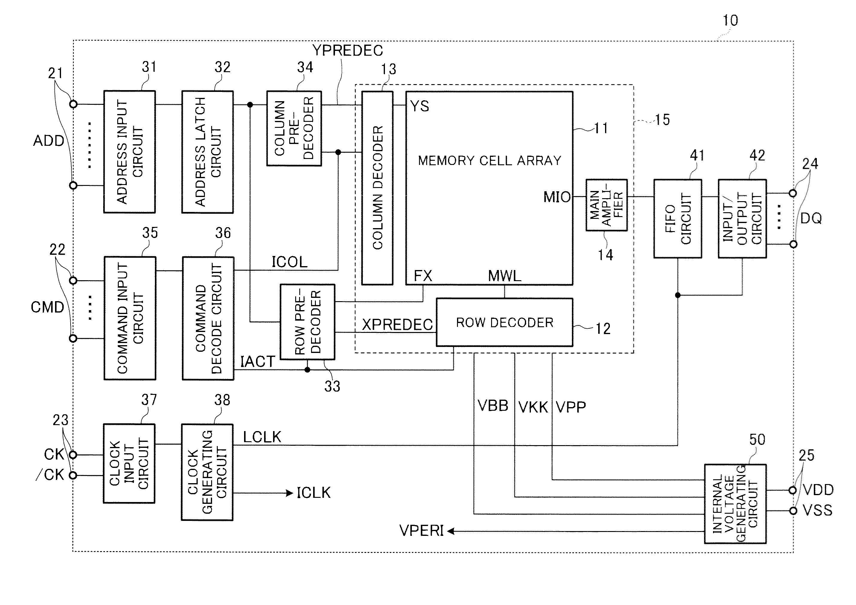
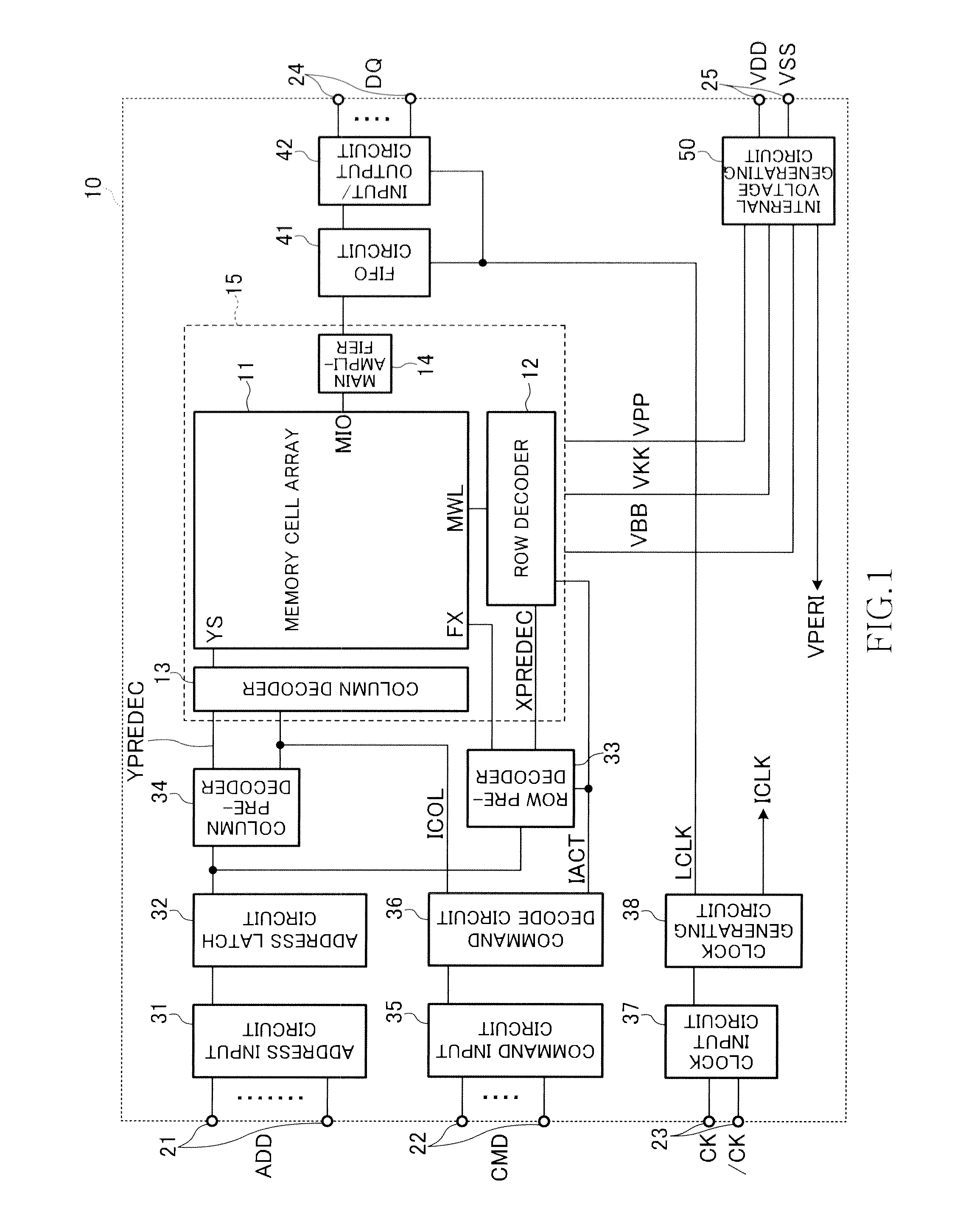
[0021]FIG. 1 is a block diagram showing an entire configuration of a semiconductor device 10 according to a first embodiment of the present invention. Referring now to FIG. 1, the semiconductor device 10 is...


PUM


Abstract

Disclosed herein is a semiconductor device that includes a signal wiring arranged on a first layer and extending over the circuit block or blocks in the first direction so as to reach the first circuit block and produce a free space above the first circuit block, the signal wiring being electrically connected to the first circuit block, a power-supply wiring arranged on a second layer and extending over the circuit block or blocks in the first direction so as to reach the first circuit block, the power-supply wiring supplying an operating voltage to the first circuit block and an auxiliary power-supply wiring being configured to enhance the operating voltage supplied by the power supply line, and the auxiliary power-supply wiring being formed in the free space produced by the arrangement of the signal wiring.

Description

BACKGROUND OF THE INVENTION[0001]1. Field of the Invention[0002]The present invention relates to a semiconductor device, and more particularly to a semiconductor device having an auxiliary power-supply wiring.[0003]2. Description of Related Art[0004]In a semiconductor device that has a plurality of functional blocks, a plurality of power-supply wiring are provided to supply operating power voltage to the functional blocks in addition to a signal wiring that is used to transmit and receive signals between the functional blocks. It is desirable that a potential that is supplied by the power-supply wiring be constant at any location on a chip. However, at a location that is distant from a power-supply circuit, the potential may decline. To mitigate such a phenomenon, what is disclosed in Japanese Patent Application Laid-Open No. 2004-273844 is a method of enhancing the power supply by forming the power-supply wirings into a mesh pattern.[0005]However, in order to form the power-supply ...

Claims


Application Information

Patent Timeline
Patent Type & Authority Applications(United States)
IPC IPC(8): G06F1/26G11C5/14
CPCG06F1/26G11C5/063G11C5/14
Inventor YOSHIMURA, MASAKINAGAMINE, HISAYUKI
Owner PS4 LUXCO SARL
Learn More