Source-down transistor with vertical field plate

a transistor and vertical field technology, applied in transistors, semiconductor devices, electrical equipment, etc., can solve the problems of affecting the efficiency of field plate placement, complex chip fabrication process, and taxing the manufacturing thermal budget, so as to improve the electric field distribution, reduce resistance, and increase the blocking voltage

Active Publication Date: 2022-05-17
DIODES INC
View PDF3 Cites 0 Cited by
  • Summary
  • Abstract
  • Description
  • Claims
  • Application Information

AI Technical Summary

Benefits of technology

[0004]In order to overcome the above mentioned technical difficulties, the Inventors invented and disclose in this paper a novel trench MOSFET structure in which the source terminal is tied to the body region and is accessible from the bottom of the chip. Each transistor cell also includes a conductive material field plate element disposed in the cell trench. The field plate element in each cell penetrates the bottom of the trench, splits a gate material into two gate electrodes, and extends into the heavily doped substrate layer where it makes electrical connection to the source of the transistor and shorts to the body region. MOSFETs with the new cell structure show improved electric field distribution in the drift region and reduced resistance and increase blocking voltage between the drain and the source of the MOSFET.

Problems solved by technology

Building transistors using wafer with four epitaxial layers and forming silicide deep down at the bottom of the trenches, as proposed by Spring, makes chip fabrication process complex and also taxes the manufacturing thermal budget.
In addition, both structures do not leave room for the placement of field plates efficiently.

Method used


Image

  • Source-down transistor with vertical field plate
  • Source-down transistor with vertical field plate
  • Source-down transistor with vertical field plate

Examples


Embodiment Construction

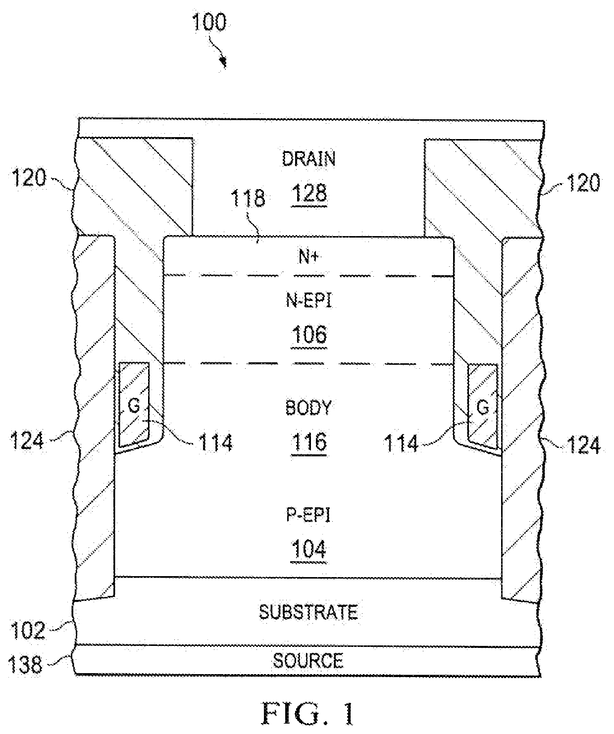
[0028]FIG. 1 depicts a cross-sectional view of a MOSFET cell 100 that embodies some aspects of this invention. The relative size of the elements depicted in FIG. 1 through FIG. 12 are not true to scale for the sake of clarity. The three terminals of the MOSFET are drain terminal 128 and the source terminal 138, and the gate terminal. The drain terminal and the source terminal are depicted in FIG. 1; the gate terminal is not depicted in FIG. 1. The gate terminal, in this example, sits on top of the chip, out of the cross sectional view depicted in FIG. 1 and is electrically connected to the gate electrode structures 114. The field plate element 124 depicted here as being electrically shorted to the source via a heavily doped substrate 102. When the gate electrode 114 is biased above a threshold voltage the P-EPI region 104 near the gate electrode inverts from p-type to n-type and forms a conductive channel. When a bias voltage is applied between the drain terminal 128 and the source ...


PUM

PropertyMeasurementUnit
conductiveaaaaaaaaaa
dielectricaaaaaaaaaa
sizeaaaaaaaaaa

Abstract

The structure of a field-effect transistor with a source-down configuration and process of making the transistor are described in this paper. The transistor is built in a semiconductor chip with a trench extending from top chip surface towards the bottom surface. The trench contains a conductive gate material embedded in a dielectric material in the trench. A conductive field plate is also embedded in the trench and extends from the top surface of the chip towards the bottom surface of the chip and splits the conductive gate electrode into two halves. The conductive field plate penetrates the trench and makes electrical contact with the heavily doped substrate near the bottom surface of the chip.

Description

BACKGROUND[0001]Vertical MOSFET device chips are commonly configured with the gate terminal and the source terminal being accessible from the top or front side of the chip and the drain terminal from the bottom or back side of the chip. This makes it convenient if additional circuit components are needed and are built close to the front side of the chip as most traditional ICs are built. In an n-channel vertical MOSFET, for example, the drain side of the transistor includes a heavily doped n-type semiconductor substrate and an n-epi layer over the substrate. The body region and the source region of the MOSFET are built at top portion of the n-epi layer close to the top of the chip.[0002]In certain applications, however, it would be desirable to have available a MOSFET in a source-down configuration. For example, in a modern DC-DC power converter circuits the drain of a first MOSFET may be directly connected to the source of a second MOSFET. Such a circuit would be easier to implemen...

Claims


Application Information

Patent Timeline
Patent Type & Authority Patents(United States)
IPC IPC(8): H01L29/78H01L29/423H01L29/40
CPCH01L29/781H01L29/407H01L29/4236H01L29/7813H01L29/41766H01L29/66734H01L29/1095H01L29/66727
Inventor CHUANG, CHIAO-SHUNLIN, CHE-YUNG
Owner DIODES INC
Why Eureka
Try Eureka