Semiconductor device

a technology of semiconductor devices and semiconductors, applied in semiconductor devices, semiconductor/solid-state device details, diodes, etc., can solve the problems of increasing chip size and insufficiently, and achieve the effect of increasing chip siz

Inactive Publication Date: 2007-07-12
ROHM CO LTD
View PDF14 Cites 2 Cited by
  • Summary
  • Abstract
  • Description
  • Claims
  • Application Information

AI Technical Summary

Benefits of technology

[0013] In order to overcome the problems described above, preferred embodiments of the present invention provide, in a semiconductor device having a plurality of power source systems, a semiconductor device that is capable of minimizing an increase in the chip size while implementing ESD damage prevention for a signal terminal of either power source system with a power supply terminal or a ground terminal of the other power source system serving as the reference potential terminal.

Problems solved by technology

Hence, in the semiconductor device, it is not sufficient merely to arrange the power source ESD protective element section in an empty space where the elements of the internal circuits and I / O circuits are not disposed.
A space for the power source ESD protective element section must be provided in addition to the space of the internal circuits and I / O circuits, which therefore causes an increase in the chip size.

Method used


Image

  • Semiconductor device
  • Semiconductor device
  • Semiconductor device

Examples


Embodiment Construction

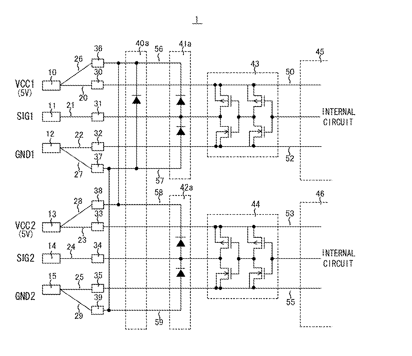
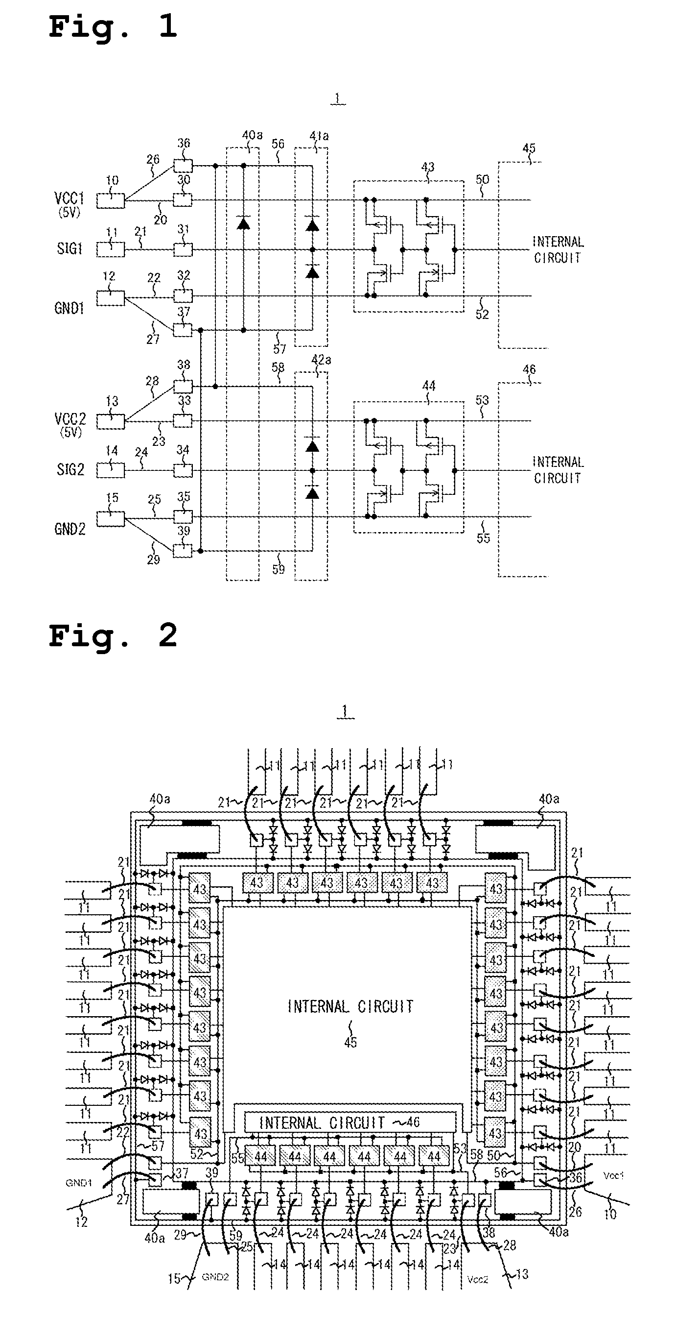
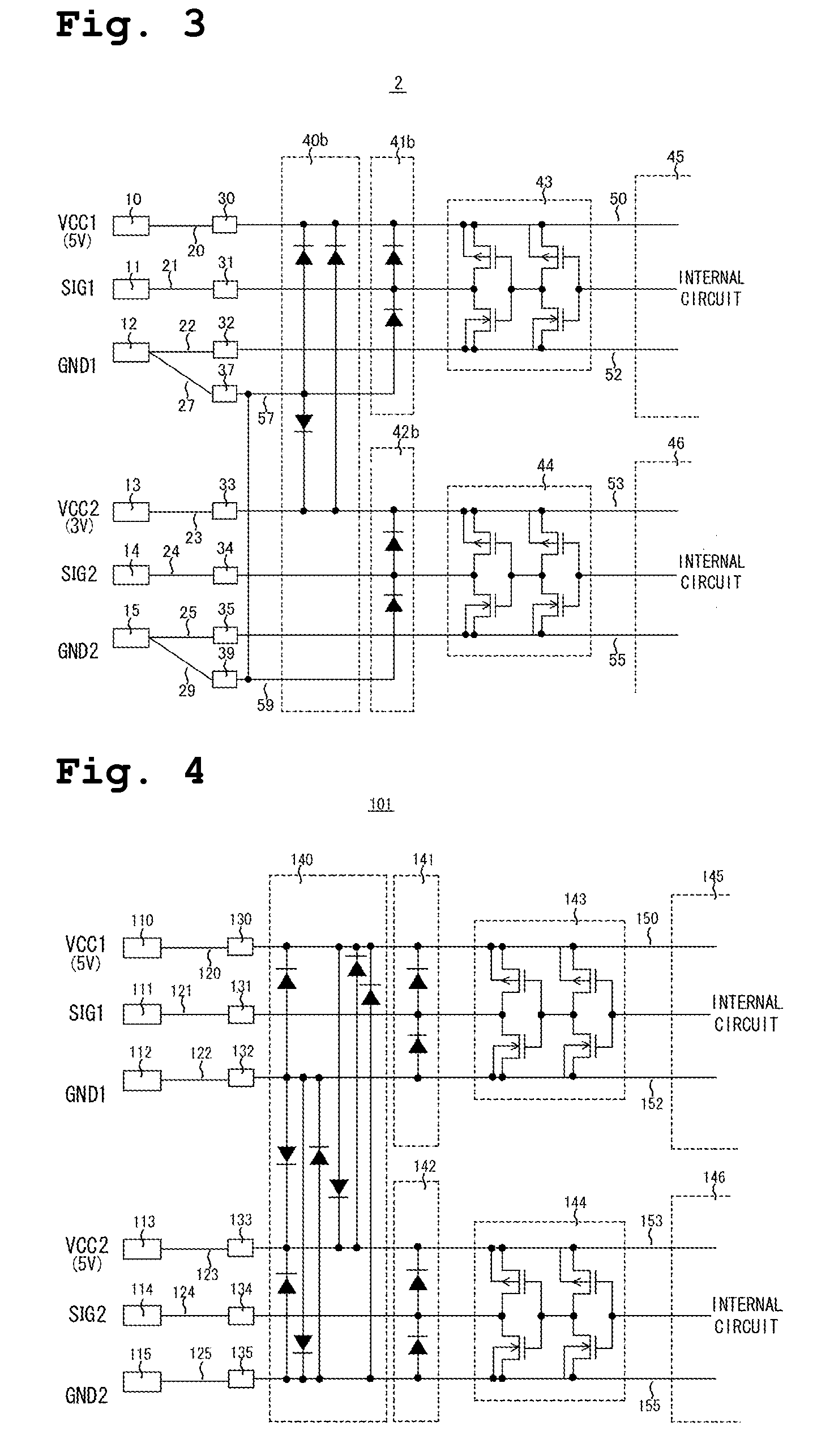
[0025] Preferred embodiments of the present invention will be described hereinbelow with reference to the drawings. FIG. 1 is a partial circuit diagram showing the connected state of each of the terminals in a semiconductor device of a first preferred embodiment of the present invention. The semiconductor device 1 has, as a plurality of power source systems, two power source systems which are a 5V digital power source system (first power source system) and a 5V analog power source system (second power source system).

[0026] The first power source system includes a power supply (VCC1) terminal 10, a ground (GND1) terminal 12, and at least one signal (SIG1) terminal 11 that inputs or outputs a signal from or to the outside of the semiconductor device 1. The second power source system includes a power supply (VCC2) terminal 13, a ground (GND2) terminal 15, and at least one signal (SIG2) terminal 14 that inputs or outputs a signal from or to the outside of the semiconductor device 1. Th...


PUM


Abstract

A semiconductor device includes, in first and second power source systems, electrostatic discharge (ESD) protective bonding pads connected by bonding wires to first and second power supply terminals and first and second ground terminals, first and second signal ESD protective element sections that are each connected to first and second signal bonding pads and the ESD protective bonding pads and protect first and second I/O circuits, respectively, and a power source ESD protective element section connected to first and second ESD protective bonding pads. The semiconductor device is capable of minimizing an increase in the chip size while implementing ESD damage countermeasures in which the power supply (or ground) terminal of one power source system serves as the reference potential terminal for the signal terminal of the other power source system.

Description

BACKGROUND OF THE INVENTION [0001] 1. Field of the Invention [0002] The present invention relates to a semiconductor device having a plurality of power source systems. [0003] 2. Description of the Related Art [0004] Conventionally, a semiconductor device having a plurality of power source systems, that is, a semiconductor device including a plurality of pairs of power supply terminals and ground terminals in which semiconductor elements are provided between the respective power supply terminal and ground terminal has utilized electrostatic discharge (ESD) countermeasures. The ESD countermeasures use all of the power supply terminals and ground terminals serving as the reference potential terminals so that there is no damage caused by ESD even when static electricity applied to a signal terminal is discharged via any of the power supply terminals and ground terminals (see, e.g., Japanese Patent Application Laid-open No. H8-148650). [0005]FIG. 4 is a partial circuit diagram showing th...

Claims


Application Information

Patent Timeline
Patent Type & Authority Applications(United States)
IPC IPC(8): H01L23/52H01L21/82H01L21/822H01L27/02H01L27/04
CPCH01L27/0255H01L2924/3011H01L2224/49175H01L2924/13091H01L2224/48091H01L2924/00014H01L2924/00H01L2224/05554H01L27/04
Inventor KATOH, TAKUMIHARA, HIDEO
Owner ROHM CO LTD
Why Eureka
Try Eureka