Semiconductor device and manufacturing method thereof

a technology of memory device and semiconductor, which is applied in the direction of semiconductor devices, electrical devices, transistors, etc., can solve the problems of affecting the down-sizing of elements for smaller geometries, difficult to fix the well at a predetermined potential, and affecting the ability of the well to perform power supply to the well, etc., to achieve the effect of facilitating the manufacture of a contact structure for the well, reducing the number of well contacts, and increasing the chip siz

Inactive Publication Date: 2005-12-01
RENESAS ELECTRONICS CORP
View PDF8 Cites 1 Cited by
  • Summary
  • Abstract
  • Description
  • Claims
  • Application Information

AI Technical Summary

Benefits of technology

[0013] According to the present invention, the well can be fixed to the predetermined potential for each memory cell. Thus, inter-memory cell well contacts become unnecessary, or the number of the well contacts can be reduced, so that the latch-up immunity of elements or transistors in particular can be improved without increase in the chip size. Further, after the impurity region of one conductivity type has been etched and removed, the power supply impurity region of the opposite conductivity type is formed. Thus, the power supply impurity region can be readily formed, and manufacture of a contact structure for performing power supply to the well is facilitated. Further, there is no need for forming a silicide layer to be deeper than the impurity region. Thus, manufacture of the contact structure is further facilitated.

Problems solved by technology

The silicide layer in other regions than the gate electrodes and the source / drain regions, in particular, becomes thicker, thereby affecting the down-sizing of elements for smaller geometries.
Thermal damage will also be caused to the elements.
It is therefore difficult to fix the well at a predetermined potential.
Thus, a special manufacturing step for formation of only the portion(s) of the silicide layer to be deeper is necessary, so that manufacturing of the semiconductor memory device therefore becomes difficult.

Method used


Image

  • Semiconductor device and manufacturing method thereof
  • Semiconductor device and manufacturing method thereof
  • Semiconductor device and manufacturing method thereof

Examples


first embodiment

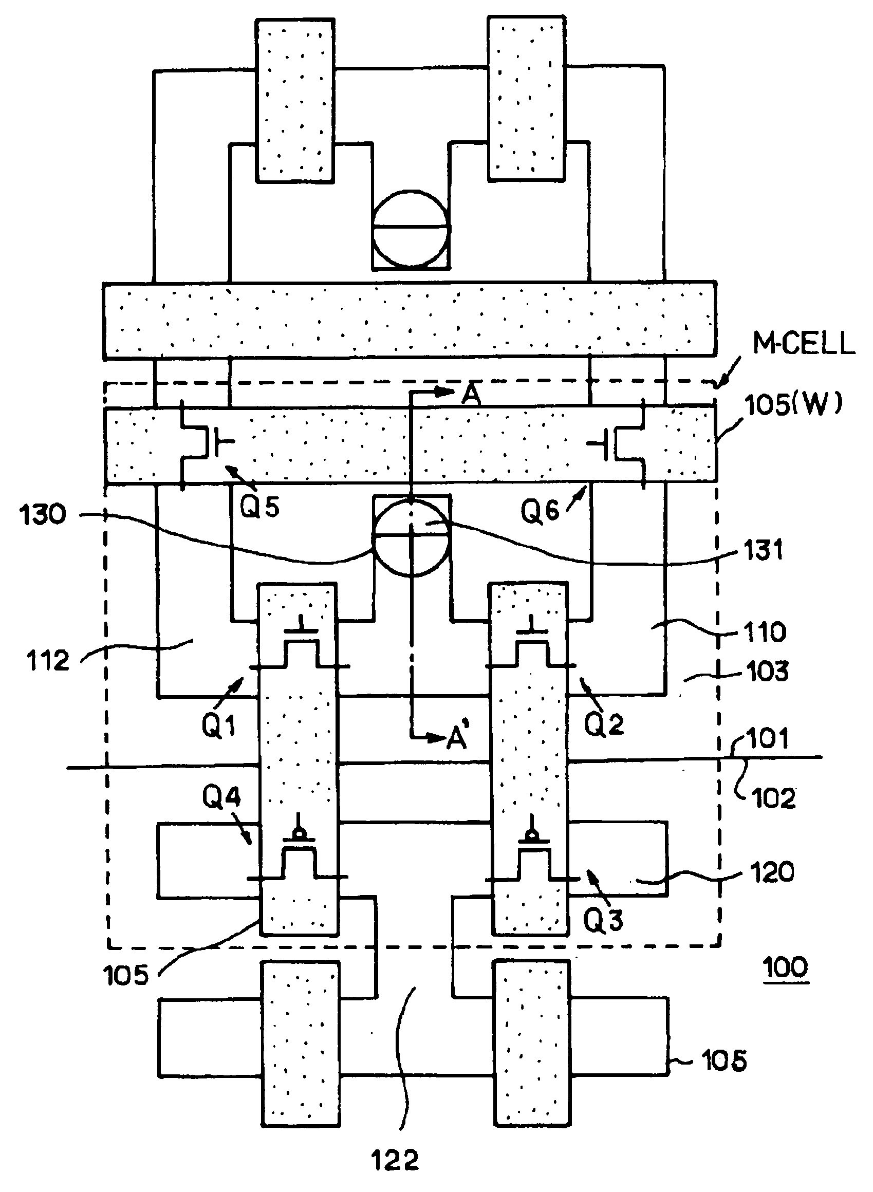
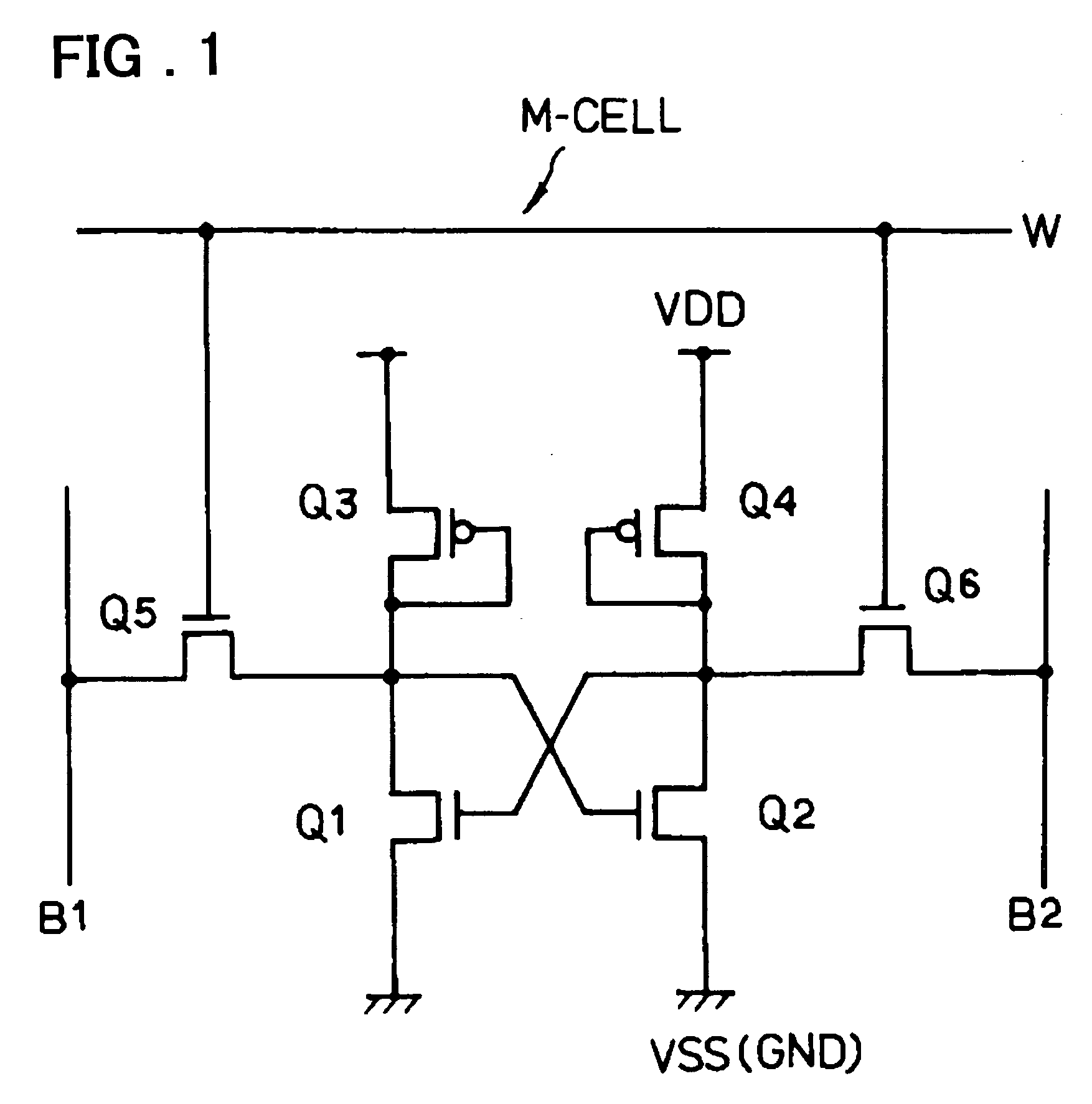
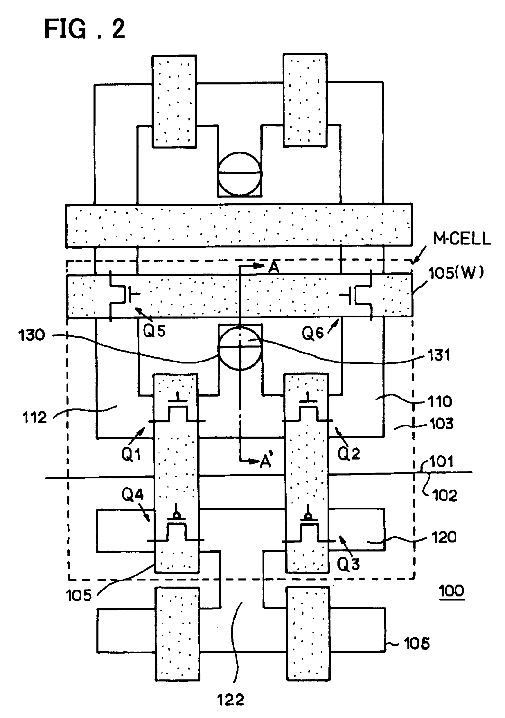
[0037] Next, embodiments of the present invention will be described with reference to the drawings. FIG. 1 is a circuit diagram of an SRAM memory cell M-CELL according to the present invention. The M-CELL is made up of driver transistors Q1 and Q2, load transistors Q3 and Q4, and transfer transistors Q5 and Q6. The driver transistors Q1 and Q2 are constituted from a pair of N-type MOS transistors with gates thereof mutually cross-connected. The load transistors Q3 and Q4 are constituted from P-type MOS transistors connected to the nodes of the driver transistors Q1 and Q2, respectively. The transfer transistors Q5 and Q6 are constituted from a pair of N-type MOS transistors connected between the node of the driver transistor Q1 and a bit line B1 and between the node of the driver transistor Q2 and a bit line B2, respectively, and with the gates thereof connected to a word line W. The load transistors Q3 and Q4 are connected to a VDD, while the driver transistors Q1 and Q2 are connec...

second embodiment

[0049]FIG. 8 is a top plan layout diagram of a second embodiment of the present invention, and FIG. 9 is a cross sectional view taken along a B-B′ line of FIG. 8. The second embodiment is an example in which the GND contact 130 is provided for the P-well 101, and a VDD contact 140 is provided for the N-well 102. Though the SRAM memory cell M-CELL has the same circuit configuration as that shown in FIG. 1, pattern shapes of the gate electrodes and the source / drain regions of the MOS transistors are different. However, the basic configuration is the same as that in the first embodiment. Thus, by assigning the same reference characters to components that are equivalent to those in the first embodiment, detailed descriptions of them will be omitted. In the second embodiment, a dummy gate 105D is formed so as to form the GND contact 130 and the VDD contact 140, and in regions adjacent to this dummy gate 105, the GND contact 130 and the VDD contact 140 are formed.

[0050] More specifically...

third embodiment

[0058]FIG. 13 is a layout diagram of an SRAM memory cell according to a third embodiment of the present invention. FIG. 14 is a cross sectional view taken along a C-C′ line in FIG. 13, and shows an example of a variation of the first embodiment. By assigning the same reference characters to components that are equivalent to those in FIGS. 2 and 3, detailed descriptions of them will be omitted. In the third embodiment, a portion of the N+ diffusion layer 112 that constitutes the source / drain region 110 of an N-type MOS transistor is etched, and the GND contact 130 is formed in this etched region. More specifically, the N− diffusion layer 111 is not etched as in the first embodiment. Then, the portion of the N+ diffusion layer 112 is etched to a depth deeper than the depth of the N+ diffusion layer 112. The P+ diffusion layer 131 is formed in this etched region, thereby forming the GND contact 130.

[0059]FIGS. 15a and 15b show cross sectional views taken in the same direction as FIG. ...


PUM


Abstract

A semiconductor device in which by fixing a well at a predetermined potential via a contact within a memory cell, latch-up immunity is improved without accompanying increase in the area of the memory cell, and of which manufacture is facilitated, and a manufacturing method thereof. In a semiconductor device including MOS transistors each having an N-type impurity region 110 formed in a P-well 101 provided in a silicon substrate 100 thereof and including a GND contact 130 for supplying a GND potential to the P-well 101, a portion of an impurity region 110 is etched and removed. Then, a P-type diffusion layer 131 for power supply is formed in the etched and removed region in the silicon substrate. Power supply to the P-well 101 is then performed via the GND contact 130 connected to the power supply diffusion layer 131.

Description

FIELD OF THE INVENTION [0001] The present invention relates to a semiconductor memory device. More specifically, the invention relates to a semiconductor memory device having an SRAM (Static Random Access Memory) and a manufacturing method thereof. BACKGROUND OF THE INVENTION [0002] In recent years, with reduction of a chip size, a PN element isolation width within an SRAM cell is reduced. As a result, the capability of a parasitic bipolar transistor is improved, so that it becomes easy to enter into a latch up state in a memory cell. In order to enter into a latch up, trigger current is necessary. However, with miniaturization of the memory cell, electrical charges caused by deterioration in SER (Soft Error Rate) immunity tend to be generated. As a measure against this, it has become a general practice to form and dispose a subcontact or a well contact for every several to several tens of memory cells, and to fix P wells at a VSS potential and fix N wells at a VDD potential. Howeve...

Claims


Application Information

Patent Timeline
Patent Type & Authority Applications(United States)
IPC IPC(8): H01L21/00H01L21/8244H01L29/41H01L27/10H01L27/11H01L29/76
CPCH01L27/1104H01L27/11H10B10/00H10B10/12
Inventor TOMIZAWA, TOMOHIRO
Owner RENESAS ELECTRONICS CORP
Why Eureka
Try Eureka