Eureka AIR delivers breakthrough ideas for toughest innovation challenges, trusted by R&D personnel around the world.

Apparatus and method for automated sort probe assembly and repair

Inactive Publication Date: 2013-10-17
INTEL CORP
View PDF13 Cites 12 Cited by
  • Summary
  • Abstract
  • Description
  • Claims
  • Application Information

AI Technical Summary

Benefits of technology

The patent text describes a system for repairing and assembling probe card substrates used in semiconductor device manufacturing. The system includes a platform and a translatable substrate for mounting and testing devices. The substrate can be repaired using a membrane probe card with electrical probes. The system automates the repair process and reduces the time and effort required for repair. The technical effects of the invention include improved efficiency and accuracy in testing and evaluating semiconductor devices, as well as reduced costs and improved reliability.

Problems solved by technology

Forming 3000 contacts which are not all at the same height and not all in the same plane is also difficult.
Similarly, assembly of probes on / in a probe card substrate is time consuming work that generally involves placing probes on the probe card substrate by hand.

Method used


Image

  • Apparatus and method for automated sort probe assembly and repair
  • Apparatus and method for automated sort probe assembly and repair
  • Apparatus and method for automated sort probe assembly and repair

Examples


Embodiment Construction

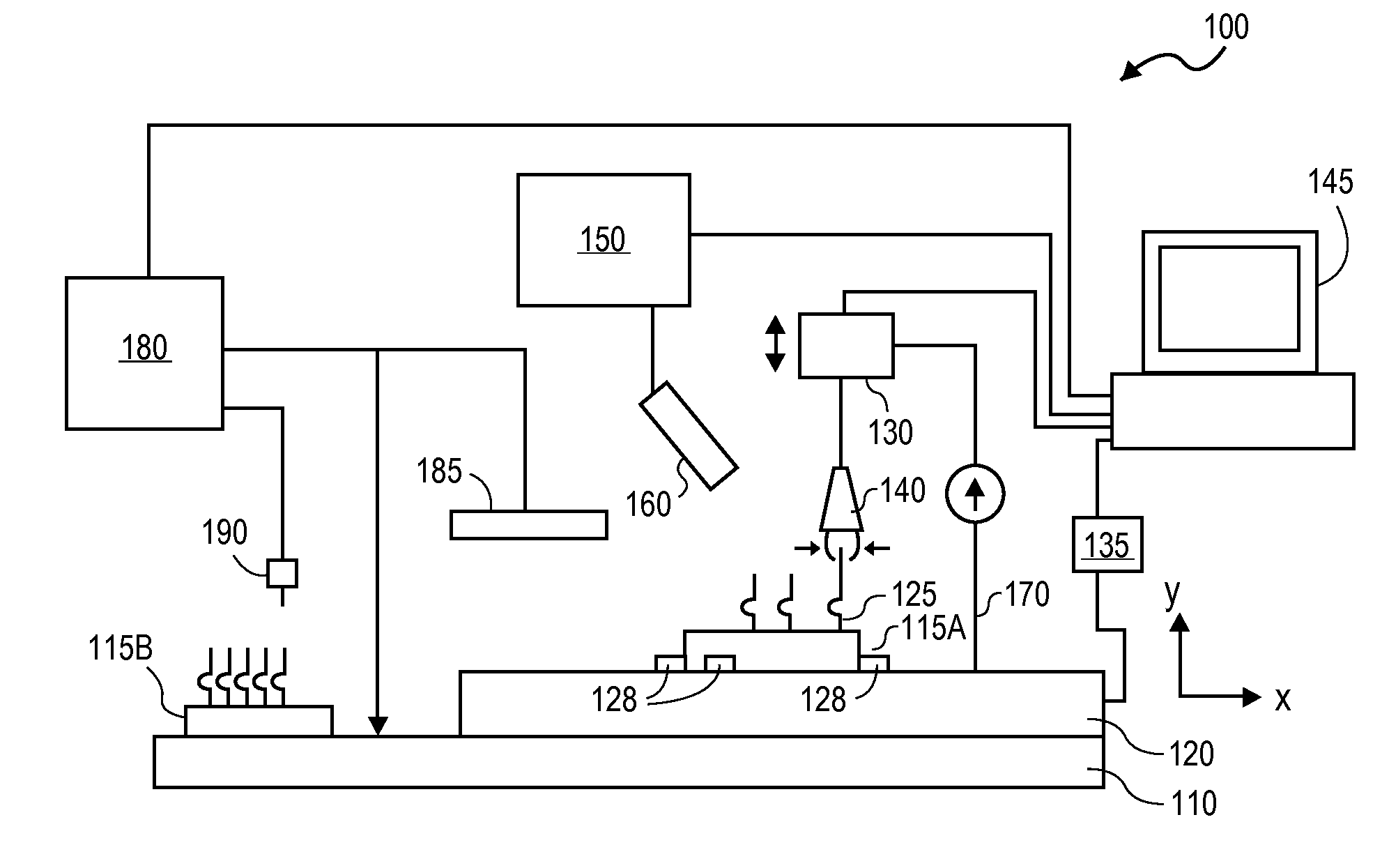
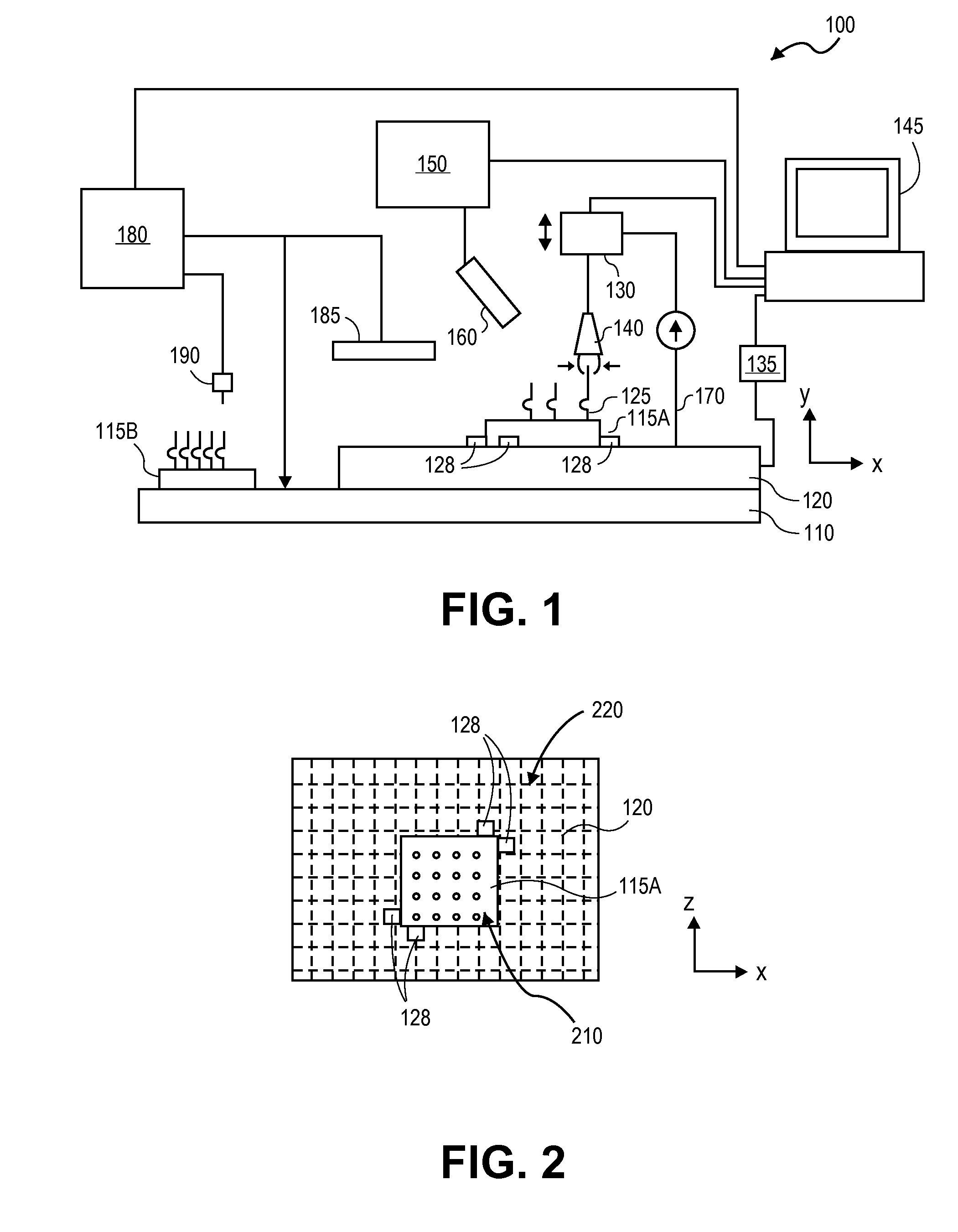
[0017]FIG. 1 shows one embodiment of a system that may be used for the automated repair of a probe card substrate such as a space transformer of a probe card and / or an assembly of a probe card substrate. System 100 includes platform 110 onto which substrate 120 is mounted. Substrate 120, in one embodiment, has a surface area that can accommodate a probe head or a full probe card. In this embodiment, substrate 120 is a substrate that is translatable in an x- and a z-direction. Representatively, substrate 120 is translatable in x and y directions according to a grid system configurable for the pitch of a probe card substrate. A representative pitch is on the order of 40 microns (μm) to 130 μm. It is appreciated that other pitches may be utilized. FIG. 2 shows a top view of substrate 120 and illustrates the xz-pitch 220 in a grid of dashed lines. Control of the translation of substrate 120 is provided by machine-readable instructions in processor 145 to which substrate 120 is connected...


PUM

PropertyMeasurementUnit
Temperatureaaaaaaaaaa
Sizeaaaaaaaaaa
Heataaaaaaaaaa

Abstract

An apparatus comprising a robot; an end effector coupled to the robot and configured to grasp or transfer a probe of a size for use in a probe card; and instructions stored on a machine readable medium coupled to the robot, the instructions comprising to configure the robot to transfer a probe to a probe card substrate or, where the probe is attached to a probe card substrate, to move the probe. A method comprising automatically transferring a probe to a probe card substrate in an assembly process or, where the probe is attached to a probe card substrate, moving the probe in a repair process; and after transferring or moving the probe, heating the probe with a heat source.

Description

BACKGROUND[0001]1. Field[0002]Sort probe assembly and repair.[0003]2. Description of Related Art[0004]In the manufacture of semiconductor devices, it is necessary that such devices be tested at the wafer level to evaluate their functionality. The process in which die in a wafer are tested is commonly referred to as “wafer sort.” Testing and determining design flaws at the die level offers several advantages. First, it allows designers to evaluate the functionality of new devices during development. Increasing packaging costs also make wafer sorting a viable cost saver, in that reliability of each die on a wafer may be tested before incurring the higher costs of packaging. Measuring reliability also allows the performance of the production process to be evaluated and production consistency rated, such as for example by “bin switching” whereby the performance of a wafer is downgraded because that wafer's performance did not meet the expected criteria.[0005]Generally, two tests are con...

Claims


Application Information

Patent Timeline
IPC IPC(8): G01R3/00
CPCG01R3/00Y10S901/02G01R1/06705G01R1/07314Y10T29/49004Y10T29/53022Y10T29/49002Y10T29/5313
Inventor ALBERTSON, TODD P.CRAIG, DAVID M.KAZA, ANILSHIA, DAVID
Owner INTEL CORP
Why Eureka
Eureka Blog
Learn More