Vernier phase to digital converter for a rotary traveling wave oscillator

Active Publication Date: 2013-10-17
PANASONIC CORP
View PDF0 Cites 8 Cited by
  • Summary
  • Abstract
  • Description
  • Claims
  • Application Information

AI Technical Summary

Benefits of technology

[0008]An apparatus and method for a high resolution Vernier phase to digital conversion circuit for a rotary traveling wave oscillator is disclosed. In one embodiment, a phase to digital conversion circuit may include an input line for conducting an input signal, the input signal having a transition and a latch having a first terminal, a second terminal and a third terminal, the first terminal of the latch coupled with the signal line for receiving the input signal. A first reference signal line for conducting a first reference signal is switchably coupled with the second terminal of the latch. A second reference signal line for conducting a second reference signal is switchably coupled with the second terminal of the latch. An output signal line is coupled with the third terminal of the latch for conducting a latched signal based on the input signal, the latched signal configured to be updated based on a transition in the first reference signal or a transition in the second reference signal.
[0009]In another embodiment, a phase to digital converter for a rotary traveling wave oscillator may include an oscillator having a closed loop transmission path. While only four signal circuit nodes are described below for the embodiment, alternative phase to digital converters for a rotary traveling wave oscillator may generally include a greater number of signal circuit nodes for tapping the oscillator. A first signal circuit node located at a first location on the transmission path for receiving a first tapped signal, a second signal circuit node located at a second location on the transmission path for receiving a second tapped signal, a third signal circuit node located at a third location on the transmission path for receiving a third tapped signal and a fourth signal circuit node located at a fourth location on the transmission path for receiving a fourth tapped signal. A first flip-flop having a first port, a second port and a third port its first port electrically connected with the first signal circuit node. A second flip-flop having a first port, a second port and a third port has its first port electrically connected with the second signal circuit node. A third flip-flop having a first port, a second port and a third port has its first port electrically connected with the third signal circuit node. A fourth flip-flop having a first port, a second port and a third port has its first port electrically connected with the fourth signal circuit node. A clocking signal circuit node is electrically connected with the second port of

Problems solved by technology

The incorporation of analog circuitry into CMOS-based devices has resulted in a variety of problems as the analog components utilized scale.
Unfortunately, traditional phase to digital converters for rotary traveling wave oscillators are forced to trade phase quantization or resolution for increased performance in the operation of the oscillators or other circuitry.
Such diminished resolution lends to inaccuracies in the precise determination of the phase component of the oscillator.
While the

Method used


Image

  • Vernier phase to digital converter for a rotary traveling wave oscillator
  • Vernier phase to digital converter for a rotary traveling wave oscillator
  • Vernier phase to digital converter for a rotary traveling wave oscillator

Examples


Embodiment Construction

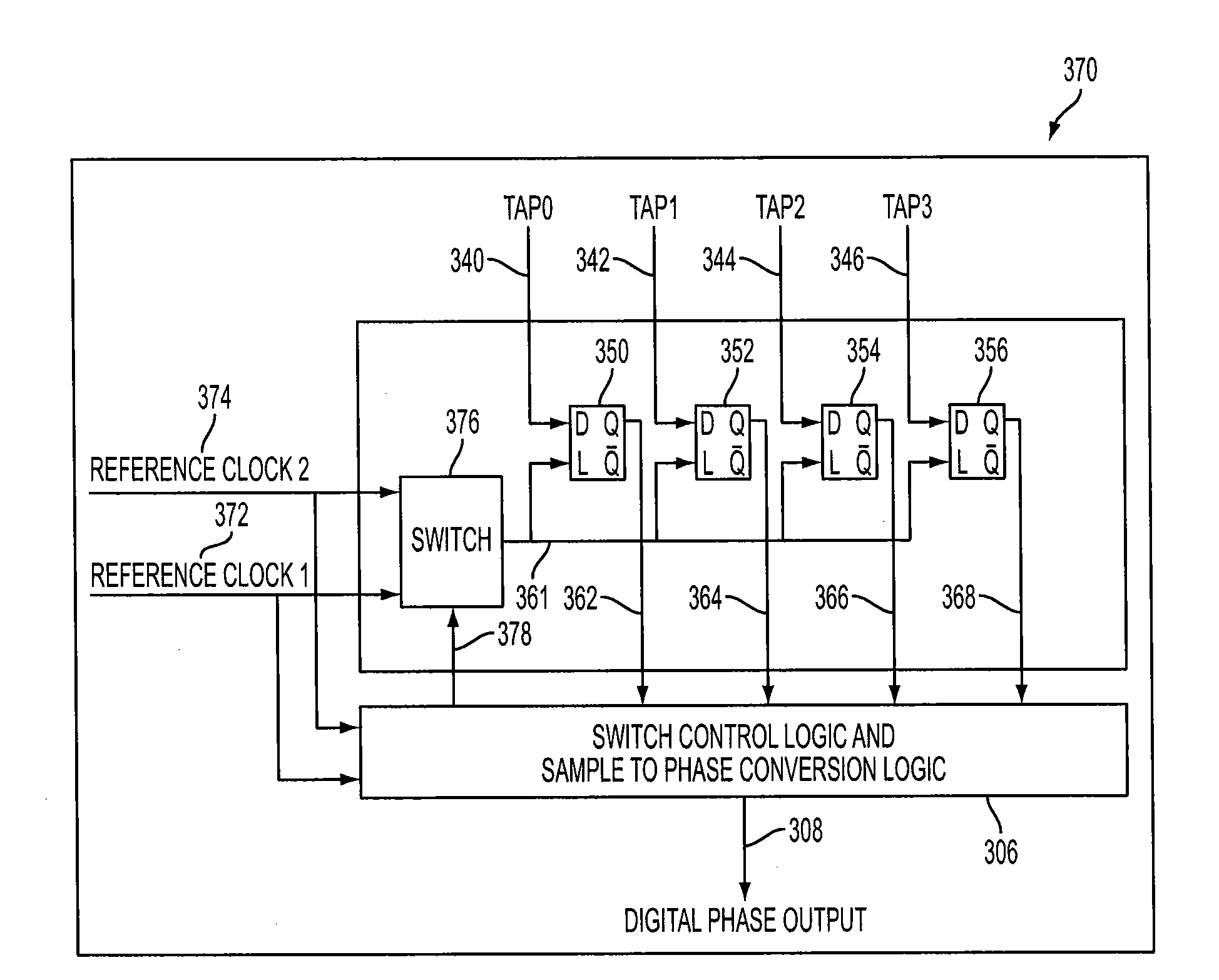
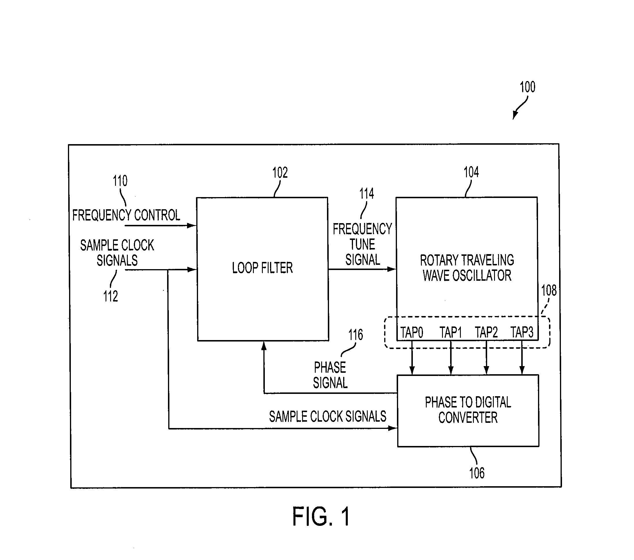
[0017]In reference to FIG. 1, a block diagram is shown of an all digital phase locked loop 100 utilizing a rotary traveling wave oscillator 104 connected with a phase to digital converter 106. All digital phase locked loops are increasingly desired as CMOS based systems and equipment become ever more prevalent in commercial and industrial applications. Traditional integration of analog phase locked loops (“PLLs”) into digital circuitry is problematic due to their susceptibility to noise and the process variations that occur during manufacturing. Digital PLLs avoid these problems and concerns. The all digital phase locked loop 100 incorporates particular phase to digital conversion circuitry for providing an increased resolution, lending to a more accurate all digital phase locked loop than may traditionally be obtained.

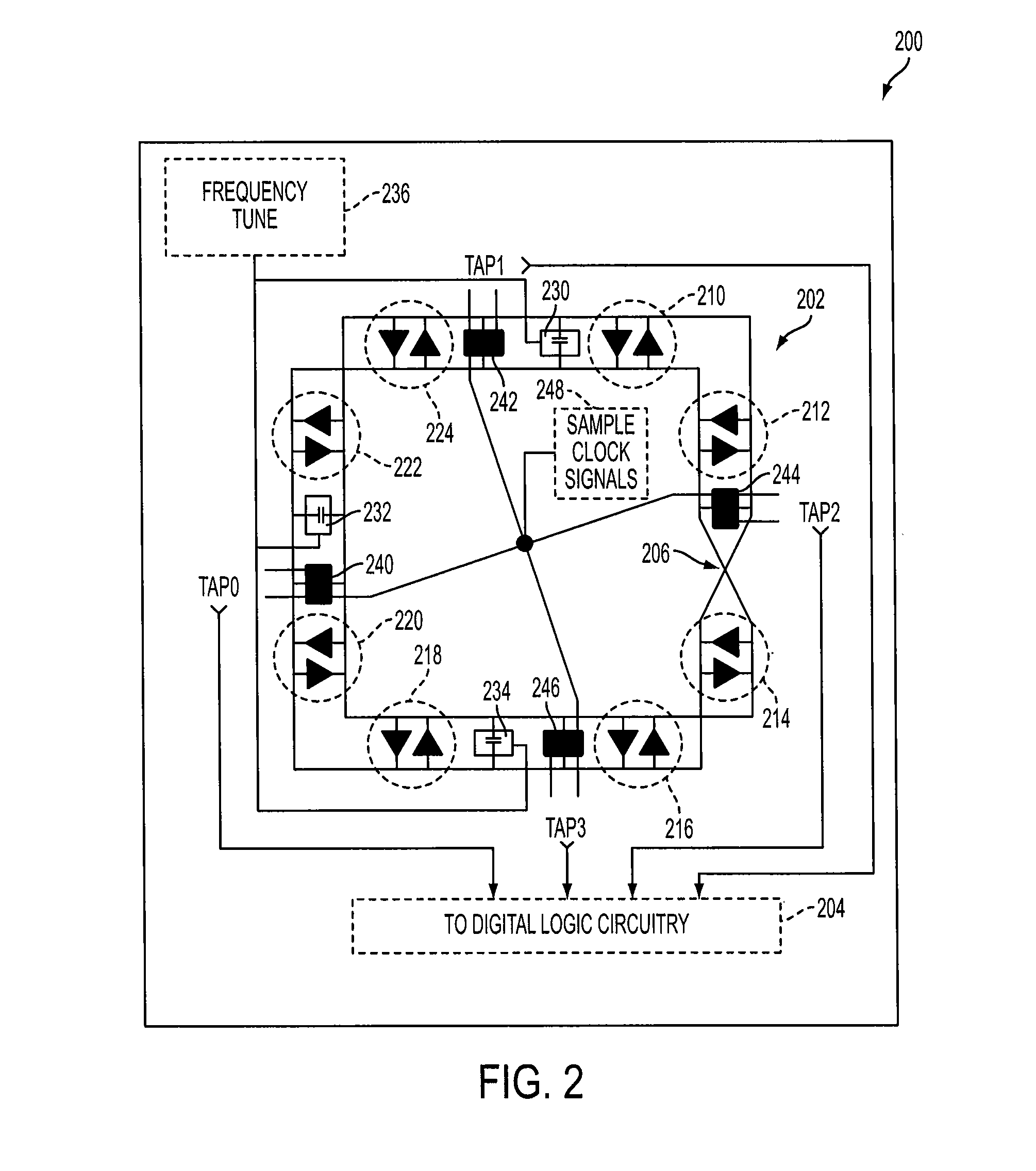
[0018]The rotary traveling wave oscillator 104 of the all digital phase locked loop 100 generates an oscillating signal that travels around a closed loop transmission...


PUM


Abstract

A phase to digital conversion circuit with improved resolution for a rotary traveling wave oscillator. The phase to digital conversion circuit connects with a closed loop transmission line via a plurality of signal lines or nodes distributed along the transmission line. As an oscillating signal propagates around the transmission line, a time waveform of the signal at each of the plurality of signal lines is transmitted to a corresponding plurality of latches. Upon a triggering condition, the plurality of latches simultaneously samples the signals from the plurality of signal lines. At least two reference clock signals are switchably coupled with the plurality of latches latch for triggering the plurality of latches based on an edge transition in each of the reference clock signals compared with an edge transition in each of the signals from the plurality of taps.

Description

BACKGROUND[0001]1. Field[0002]The present invention relates generally to improvements in phase to digital conversion circuits and more particularly pertains to higher resolution Vernier phase to digital converters for rotary traveling wave oscillators and improvements thereto.[0003]2. Description of the Related Art[0004]The incorporation of analog circuitry into CMOS-based devices has resulted in a variety of problems as the analog components utilized scale. Many times, a particular device design must be redone for each new analog technology sought to be used. Digital circuitry on the other hand has resulted in far fewer issues since digital designs generally scale with the technology. Thus, it is becoming increasingly popular to replace as much analog circuitry as possible with digital equivalents. Radio frequency circuits, such as phase locked loops, particularly benefit from the use of all digital components.[0005]One type of all digital phase locked loop utilizes a rotary travel...

Claims


Application Information

Patent Timeline
IPC IPC(8): H03L7/06
CPCH03L7/0996
Inventor BOOTH, RICHARD W. D.TAKINAMI, KOJI
Owner PANASONIC CORP
Why Eureka
Try Eureka