Circuit module and method of manufacturing the same

a technology of circuit modules and circuit modules, applied in the direction of printed circuit non-printed electric components, electrical apparatus contruction details, and semiconductor/solid-state device details, etc., can solve the problems of difficult to achieve stable shield function, difficult to reduce the thickness of the circuit module, and potential damage to the connection parts

Inactive Publication Date: 2013-10-17
TAIYO YUDEN KK
View PDF2 Cites 26 Cited by
  • Summary
  • Abstract
  • Description
  • Claims
  • Application Information

AI Technical Summary

Benefits of technology

[0009]In light of the aforementioned situation, an object of the present invention is to provide a circuit module that ...

Problems solved by technology

With the circuit module described in Patent Literature 1, however, the top shield layer and each shield plate are connected only at the top face of the insulation resin layer, which leads to a potential risk of damage to these connection parts if thermal stress or other stress is applied to the top face in parallel direction.
Such dama...

Method used


Image

  • Circuit module and method of manufacturing the same
  • Circuit module and method of manufacturing the same
  • Circuit module and method of manufacturing the same

Examples


first embodiment

[Circuit Module]

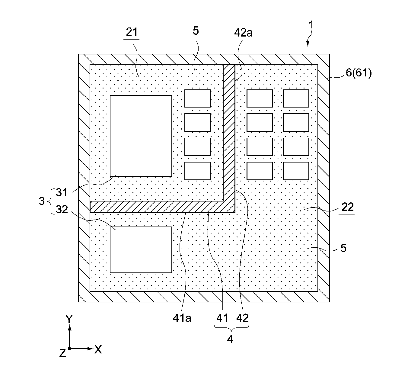
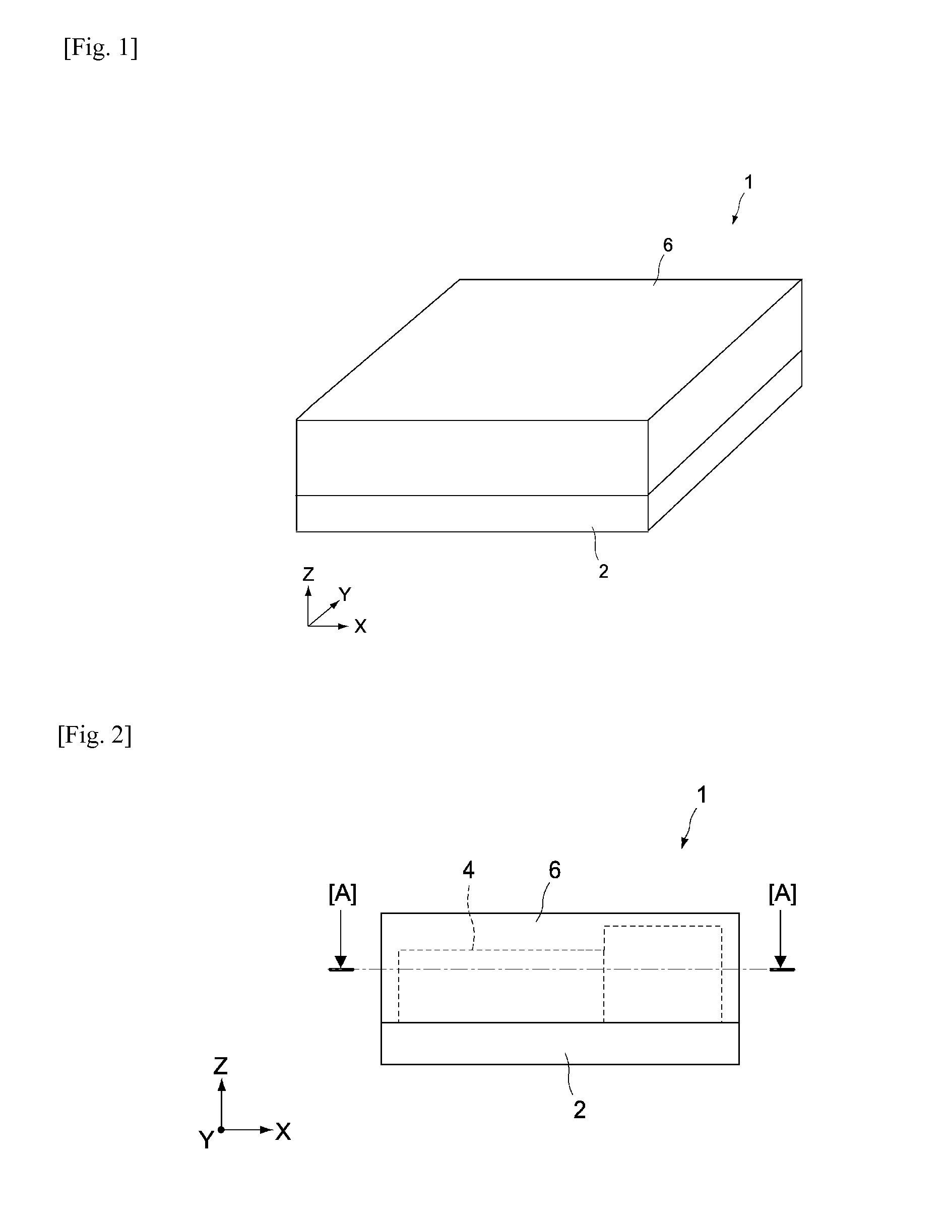
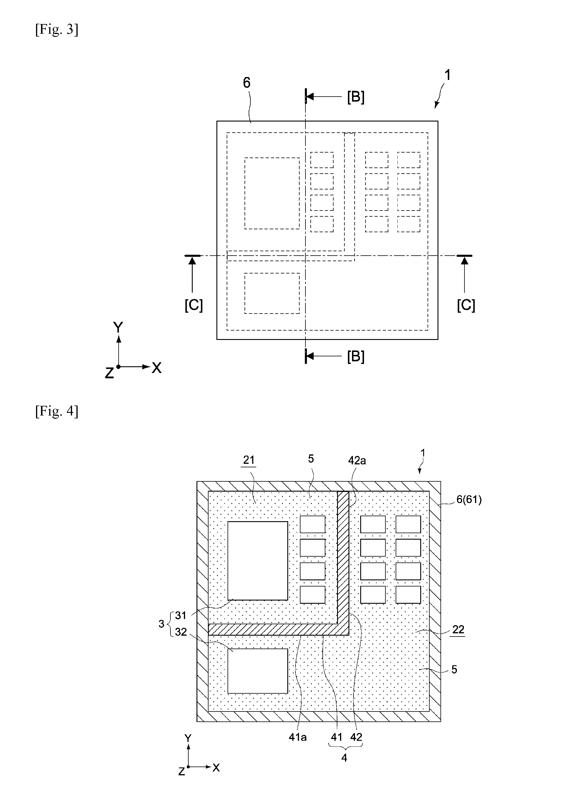
[0084]FIGS. 1 to 3 are schematic views showing the exterior of a circuit module pertaining to an embodiment of the present invention, where FIG. 1 is a perspective view, FIG. 2 is a front view, and FIG. 3 is a plan view. On the other hand, FIG. 4 is a section view of FIG. 2 cut along line [A]-[A], FIG. 5(A) is a section view cut along line [B]-[B], and FIGS. 5(B) and (C) are enlarged views showing key parts of FIG. 5(A). FIG. 6 is a section view of FIG. 3 cut along line [C]-[C].

[0085]In each drawing, the X, Y and Z axes represent three axis directions that are mutually orthogonal, where the Z-axis direction corresponds to the thickness direction of the circuit module. To facilitate understanding, the constitution of each part is exaggerated.

[0086]The circuit module 1 pertaining to this embodiment has a board 2, multiple electronic components 3, a shield member 4, sealing layer 5, and cover layer 6.

[0087]The circuit module 1 is constituted to have an overall shape of ...

second embodiment

[0141]FIGS. 14 to 16 illustrate the second embodiment of the present invention. This embodiment is explained by focusing on those portions different from the first embodiment, and those portions similar to the constitution and effects of the first embodiment are either not explained or explained in a simple way.

[0142]In this embodiment, the step to form the groove to be filled by the first cover part 61 of the cover layer 6 is different from the first embodiment mentioned above. FIG. 14(A) is a top view of the board assembly 25 showing the groove forming step, FIG. 14(B) is a section view of key parts as viewed in the Y-axis direction, FIG. 15 is a section view of key parts of the circuit module after forming of the cover layer as viewed in the Y-axis direction, and FIG. 16 is a section view of key parts showing the shape of the groove.

[0143]The circuit module pertaining to this embodiment has a groove 510 formed with a dicer on the top face of the sealing layer 5. The groove 510 is...


PUM

PropertyMeasurementUnit
Electrical conductoraaaaaaaaaa
Areaaaaaaaaaaa
Heightaaaaaaaaaa

Abstract

A circuit module pertaining to an embodiment of the present invention has a board, multiple electronic components, a shield member, sealing layer, and cover layer. The board has a mounting surface that includes a first area and second area in which the multiple electronic components are mounted. The shield member is constituted by conductive material and placed between the first area and second area on the mounting surface. The sealing layer has on its top surface a groove having its bottom face including an upper end face of the shield member, is formed on the mounting surface, and is constituted by an insulator that covers the multiple electronic components. The cover layer is constituted by conductive material and has a first cover part that fills the groove as well as a second cover part that covers the first cover part and sealing layer.

Description

BACKGROUND [0001]1. Field of the Invention[0002]The present invention relates to a circuit module with electromagnetic shield function, as well as a manufacturing method thereof.[0003]2. Description of the Related Art[0004]Circuit modules comprising multiple electronic components mounted on a board, which are installed in various types of electronic equipment, are known. These circuit modules generally adopt a constitution whereby electromagnetic shield function is provided to prevent electromagnetic waves from leaking to the outside of the module or entering from the outside.[0005]In addition, various ingenious ideas are being proposed to prevent electromagnetic interference between these multiple electronic components, as the types of electronic components mounted in circuit modules become increasingly diverse. For example, Patent Literature 1 describes a circuit module having a top shield layer, side shield plates that surround a module board, and an intermediate shield plate pla...

Claims


Application Information

Patent Timeline
IPC IPC(8): H05K9/00H05K13/00
CPCH05K9/0084H05K13/0046H01L23/552H01L24/97H01L2924/15192H05K5/0095H05K9/0037H05K1/0218H05K3/284H05K2201/09972H05K2201/10371H01L2924/1461H01L2924/351H01L2924/12042Y10T29/49146H01L2924/00H05K9/00H05K1/02H05K13/00
Inventor SHIMAMURA, MASAYAMUGIYA, EIJI
Owner TAIYO YUDEN KK
Why Eureka
Try Eureka