

Reactor for Atomic Layer Deposition (ALD), Application to Encapsulation of an OLED Device by Deposition of a Transparent Al2O3 Film
a technology of atomic layer and reactor, applied in the direction of coatings, electroluminescent light sources, electric lighting sources, etc., can solve the problems of device deformation, inability to use, appearance of non-emissive dark spots, etc., and achieve the effect of preventing or preventing the contamination of the substrate by particles
- Summary
- Abstract
- Description
- Claims
- Application Information
AI Technical Summary
Benefits of technology
Problems solved by technology
Method used
Image

Examples
Embodiment Construction
[0043]Other advantages and features of the invention will become apparent on reading the detailed description of the invention given by way of nonlimiting illustration and with reference to the following figures in which:
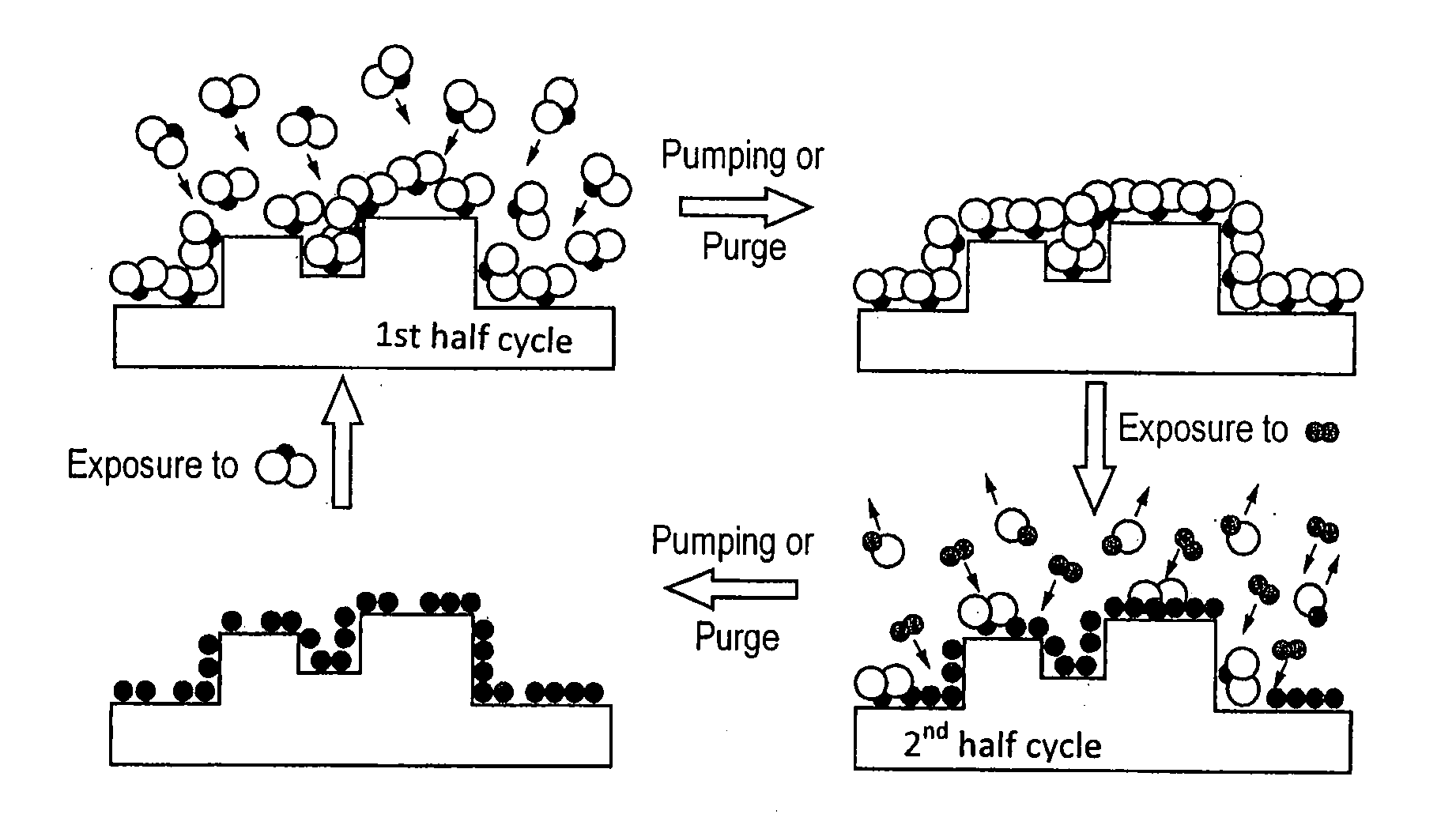
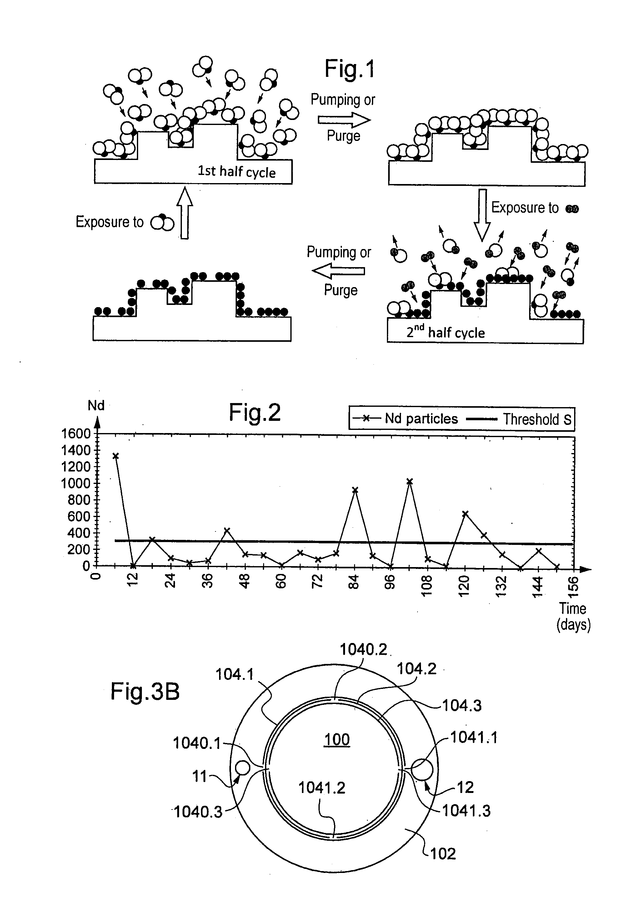
[0044]FIGS. 1 and 2 have already been commented upon above in the preamble. They are therefore not described in greater detail here.
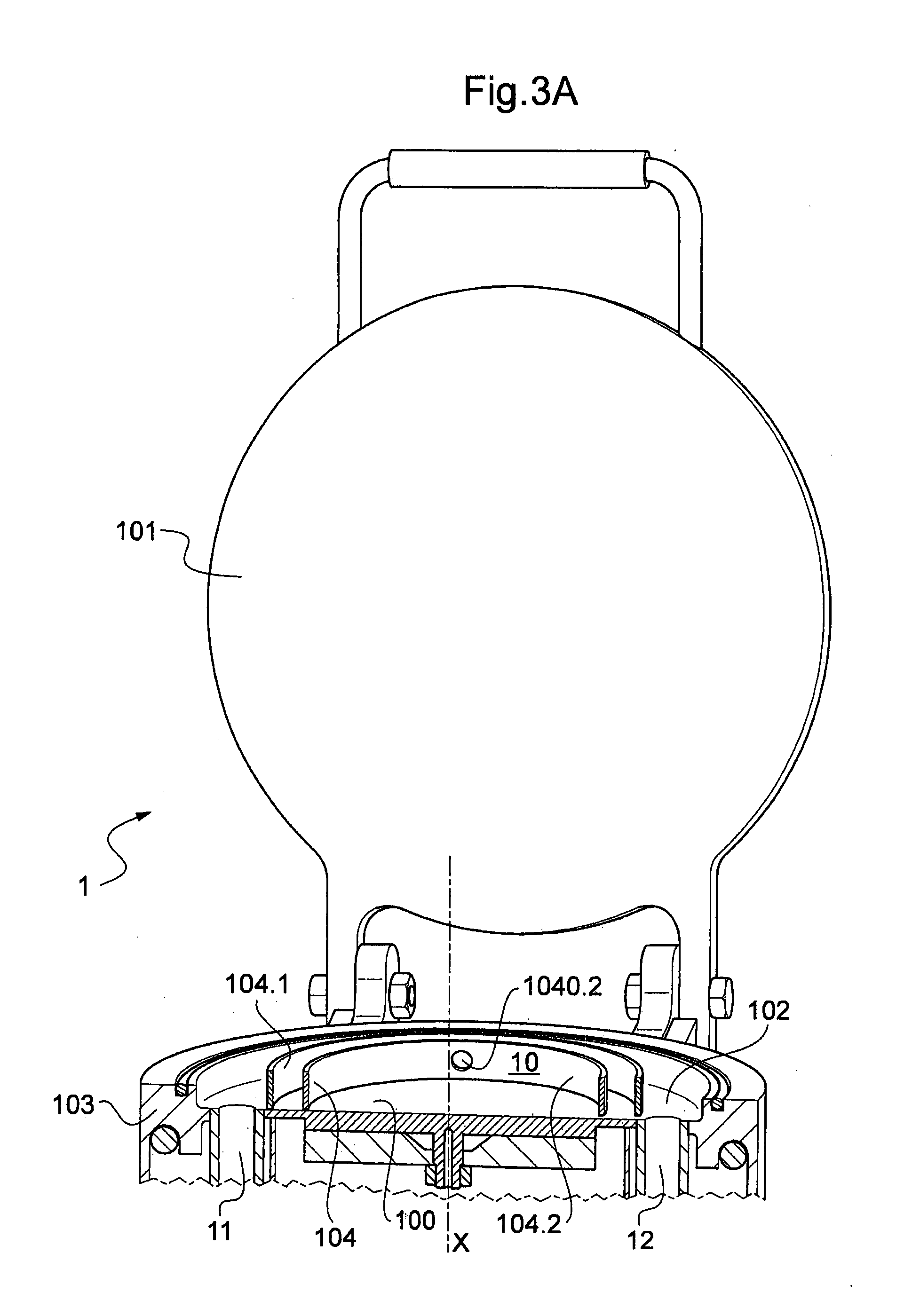
[0045]FIGS. 3A and 3B show an ALD reactor 1 according to the invention. For the sake of clarity, only two apertured walls 104.1, 104.2 according to the invention have been shown in FIG. 3A.
[0046]The ALD reactor 1 according to the invention comprises a reaction chamber 10 having a generally cylindrical shape about its longitudinal X-axis, this reaction chamber comprising a platen 100 and being bounded by a lid 101 that forms the upper surface, a base 102 that forms the lower surface and a sidewall 103 having a generally annular shape. As shown in the open position in FIG. 3A, the lid 101 opens by pivoting about a horizontal axis and thus...
PUM
| Property | Measurement | Unit |
|---|---|---|
| angle | aaaaa | aaaaa |
| width | aaaaa | aaaaa |
| width | aaaaa | aaaaa |
Abstract
Description
Claims
Application Information