Image sensor package

Active Publication Date: 2013-10-31
HUAWEI TECH CO LTD
View PDF7 Cites 27 Cited by
  • Summary
  • Abstract
  • Description
  • Claims
  • Application Information

AI Technical Summary

Benefits of technology

[0034]In accordance with an exemplary embodiment of the image sensor package, the image sensor package can enhance the reliability thereof with respect to physical impact while the slenderization thereof may be possible by changing the material and/or the structure of the substrate, at which an image sensor chip is mounted, in the structure of the ima

Problems solved by technology

The Chip-On-Board method has a high cost of production due to a wire bonding process.
Thus, producing a slenderized image sensor package is difficult.
However, the image sensor

Method used


Image

  • Image sensor package
  • Image sensor package
  • Image sensor package

Examples


Example

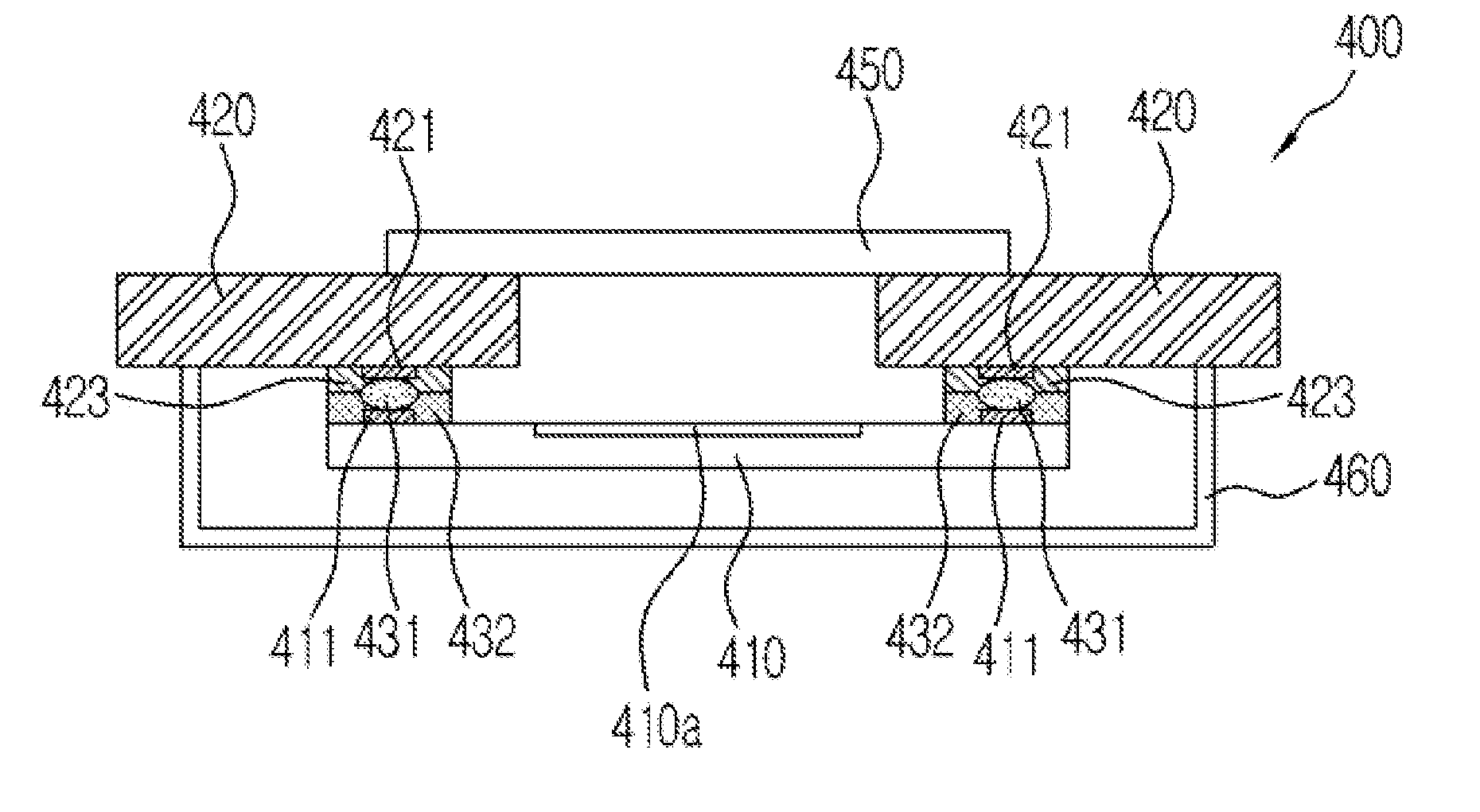
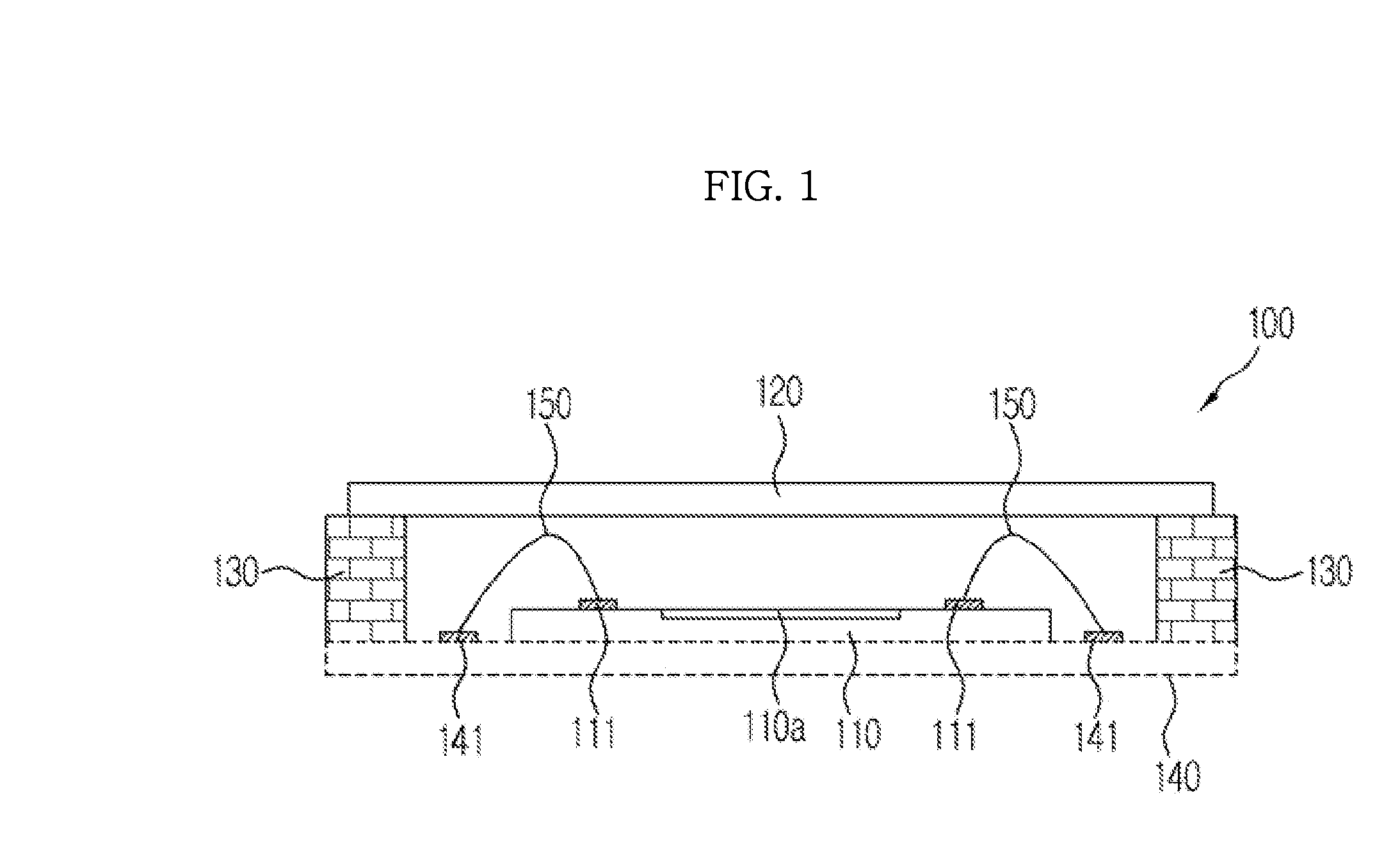
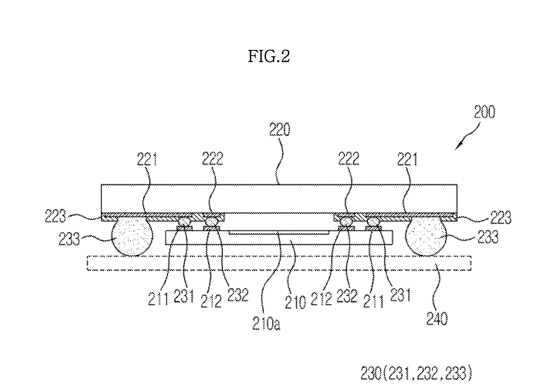
[0042]Reference will now be made in detail to the embodiments of the present disclosure, examples of which are illustrated in the accompanying drawings, wherein like reference numerals refer to like elements throughout.

[0043]FIG. 3 is a cross-sectional view of an image sensor package in accordance with an embodiment of the present disclosure.

[0044]As illustrated on FIG. 3, an image sensor package 300 in accordance with an embodiment of the present disclosure includes an image sensor chip 310, a substrate 320 disposed at an upper side of the image sensor chip 310 so as to be flip-chip bonded to the image sensor chip 310, a printed circuit board 340 at which the substrate 320 provided with the image sensor chip 310 bonded thereto is mounted, a solder part 330 configured to electrically connect the substrate 320 provided with the image sensor chip 310 mounted thereto to the printed circuit board 340, and a transparent substrate 350 on which glass-like material having , for example, an ...


PUM


Abstract

An image sensor package and image sensor chip capable of being slenderized while enhancing the reliability with respect to physical impact are provided. The image sensor package includes an image sensor chip provided with a pixel domain at a central portion of an upper surface thereof, a substrate disposed at an upper side of the image sensor chip so as to be flip-chip bonded with respect to the image sensor chip, provided with a hole formed at a position corresponding to the pixel domain, and formed of organic material, a printed circuit board at which the substrate provided with the image sensor chip bonded thereto is mounted, and a solder ball configured to electrically connect the substrate to the printed circuit board.

Description

CROSS-REFERENCE TO RELATED APPLICATIONS[0001]This application is related to, and claims priority to, the Korean Patent Application No. 10-2012-0043146, filed on Apr. 25, 2012, in the Korean Intellectual Property Office, the disclosure of which is incorporated herein by reference.BACKGROUND[0002]1. Field[0003]Embodiments of the present disclosure relate to an image sensor package.[0004]2. Description of the Related Art[0005]An image sensor may be a semiconductor device configured to detect information on a subject and to convert the detected information into an electrical image signal. An image sensor may be installed in a digital camera or a camcorder, as well as in a tablet PC or a mobile phone. Thus, the market thereof is rapidly expanding. The image sensor may include a CCD (Charge Coupled Device) and / or a CMOS (Complementary Metal Oxide Silicon).[0006]Optical electronics device such as the image sensor may be packaged so as to be connectable to a higher-level package such as a l...

Claims


Application Information

Patent Timeline
IPC IPC(8): H01L27/146
CPCH01L27/14636H01L27/14618H01L2224/16225H01L2224/48091H01L2224/48227H01L2924/00014H01L27/146
Inventor PARK, TAE SANGSHIN, HYO YOUNG
Owner HUAWEI TECH CO LTD
Why Eureka
Try Eureka