Method and system for wafer and strip level batch die attach assembly

a batch die and assembly technology, applied in the field of semiconductor die assembly packaging, can solve the problems of a significant percentage of the die size of the lateral placement error, the die attaching process has limited control of the rotation accuracy of the die, and the process is expensive in both time and resources

Inactive Publication Date: 2013-10-31
FREESCALE SEMICON INC
View PDF5 Cites 20 Cited by
  • Summary
  • Abstract
  • Description
  • Claims
  • Application Information

AI Technical Summary

Problems solved by technology

This process is costly in both time and resources.
The die attach process has limited control of die rotation accuracy, which is often not sufficient for certain sensor applications such as accelerometers and magnetometers.
In addition, as die geometries get smaller, any lateral placement errors can be a significant percentage of the die size.
Thus, the traditional die attach processes cannot meet the tolerances of smaller and more sensitive stacked devices.

Method used


Image

  • Method and system for wafer and strip level batch die attach assembly
  • Method and system for wafer and strip level batch die attach assembly
  • Method and system for wafer and strip level batch die attach assembly

Examples


Embodiment Construction

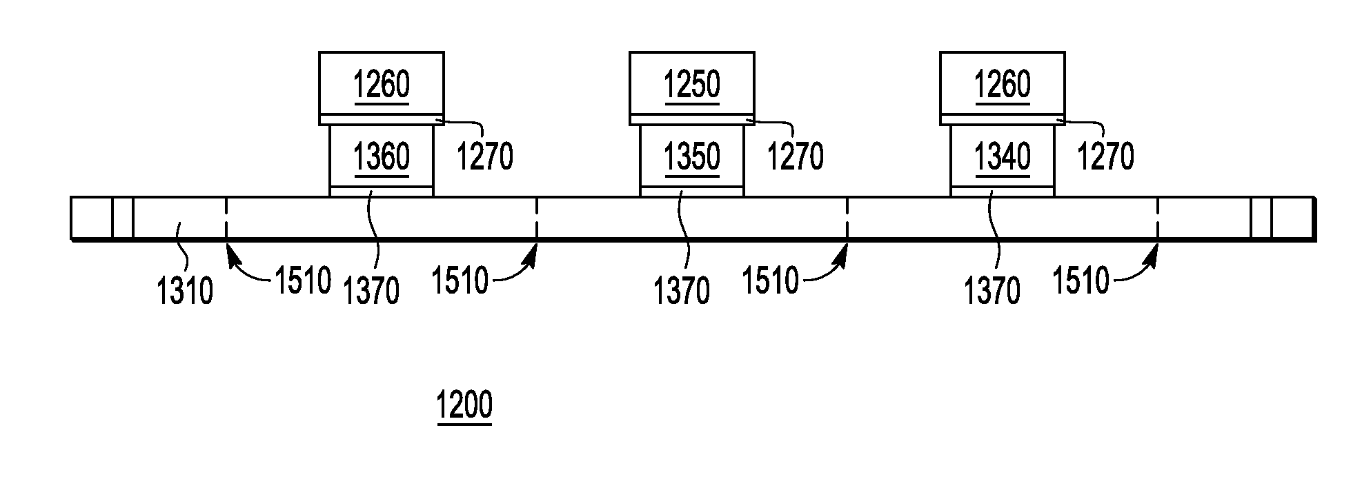
[0026]Embodiments of the present invention provide a method and system by which multiple die stacks can be assembled in a batch manner, and which also provides for die alignment tolerances required by MEMS and other SIP applications. The batch process and accuracy is provided, in part, by an intermediate die attach carrier that has multiple die pockets fabricated to hold a set of die with an alignment required for the application. Die are placed in each pocket using a die sorting process. Then a batch process operation is performed in which wafer or strip-level alignment and bonding tools are used to join the die in the intermediate die attach carrier in stacks with a second set of die.

[0027]Stacking die in package assemblies has historically been a difficult and expensive process. Many products, including sensor products, require multi-die assembly and high angular accuracy. Current processes for providing stacked die assembly include using conventional die attach equipment in a on...


PUM

PropertyMeasurementUnit
of angleaaaaaaaaaa
anisotropicaaaaaaaaaa
pressureaaaaaaaaaa

Abstract

A method and system is provided by which multiple semiconductor die stacks can be assembled in a batch manner, and which also provides for die alignment tolerances required by microelectromechanical systems and other system-in-package applications. The batch process and accuracy is provided, in part, by an intermediate die attach carrier that has multiple die pockets fabricated to hold a set of die with an alignment required for the application. Die are placed in each pocket using a die sorting process. Then a batch process operation is performed in which wafer or strip-level alignment and bonding tools are used to join the die in the intermediate die attach carrier in stacks with a second set of die.

Description

BACKGROUND[0001]1. Field[0002]This disclosure relates generally to semiconductor packaging, and more specifically, to stacked semiconductor die assembly packaging using batch processing.[0003]2. Related Art[0004]Size and processing needs for modern electronic devices result in placing larger numbers of semiconductor components in progressively smaller areas. One mechanism for addressing these space concerns is to stack semiconductor die within a package, thereby providing additional “real estate” for components in a system-in-a-package (SIP). Additionally, varying types of microelectromechanical systems (MEMS) devices also use stacking processes in order to provide a physically close relationship between a sensor portion of the MEMS device and a signal processing portion of the MEMS device.[0005]Typical processes for assembling stacked die in a package provide for one-by-one placement of a die on another die, using die attach equipment. This process is costly in both time and resour...

Claims


Application Information

Patent Timeline
Patent Type & Authority Applications(United States)
IPC IPC(8): H01L23/488B32B3/26H01L21/78
CPCH01L24/83H01L24/95H01L2224/32145H01L2224/48091H01L2224/48145H01L2224/73265H01L2924/10253H01L24/32H01L24/48H01L24/73H01L2224/32225H01L2224/48227H01L2224/83001H01L2224/83191H01L2924/00014B81C3/005B81C99/002B81C2203/054H01L25/0657H01L25/50H01L2224/94H01L2224/97H01L2225/0651H01L2225/06506H01L2225/06568H01L2924/01322H01L2924/1461H01L2924/181H01L2924/12042H01L2224/48147Y10T428/24479H01L2924/00H01L2224/45099H01L2224/83H01L2924/00012
Inventor HAN, CALEB C.
Owner FREESCALE SEMICON INC
Why Eureka
Try Eureka