Electronic device for radiofrequency or power applications and process for manufacturing such a device

a technology of radiofrequency or power applications and electronic devices, applied in the direction of printed circuits, printed circuit non-printed electric components association, electrical apparatus, etc., can solve the problems of poor heat conductivity, and low thermal conductivity of substrates

Active Publication Date: 2013-11-07
SOITEC SA
View PDF7 Cites 77 Cited by
  • Summary
  • Abstract
  • Description
  • Claims
  • Application Information

AI Technical Summary

Benefits of technology

[0032]Another object of the invention is a process for manufacturing a device for radiofrequency or power applications, comprising a layer supporting electronic components on a support substrate, the process comprising the following successive steps:
[0032]Another object of the invention is a process for manufacturing a device for radiofrequency or power applications, comprising a layer supporting electronic components on a support substrate, the process comprising the following successive steps:

Problems solved by technology

However, these substrates involve the drawback of having a low thermal conductivity, particularly due to the presence of a relatively thick layer of silicon oxide (SiO2), which is a poor heat conductor.
The thermal conductivity of such SOI substrates, since the oxide thickness exceeds about 50 nm, may then be limited by the conductivity of this silicon oxide, of the order of 1 to 2 W / m K, which is insufficient for the intended applications.
Moreover, sapphire substrates are relatively costly, particularly for diameters larger than 150 mm.

Method used


Image

  • Electronic device for radiofrequency or power applications and process for manufacturing such a device
  • Electronic device for radiofrequency or power applications and process for manufacturing such a device
  • Electronic device for radiofrequency or power applications and process for manufacturing such a device

Examples


Embodiment Construction

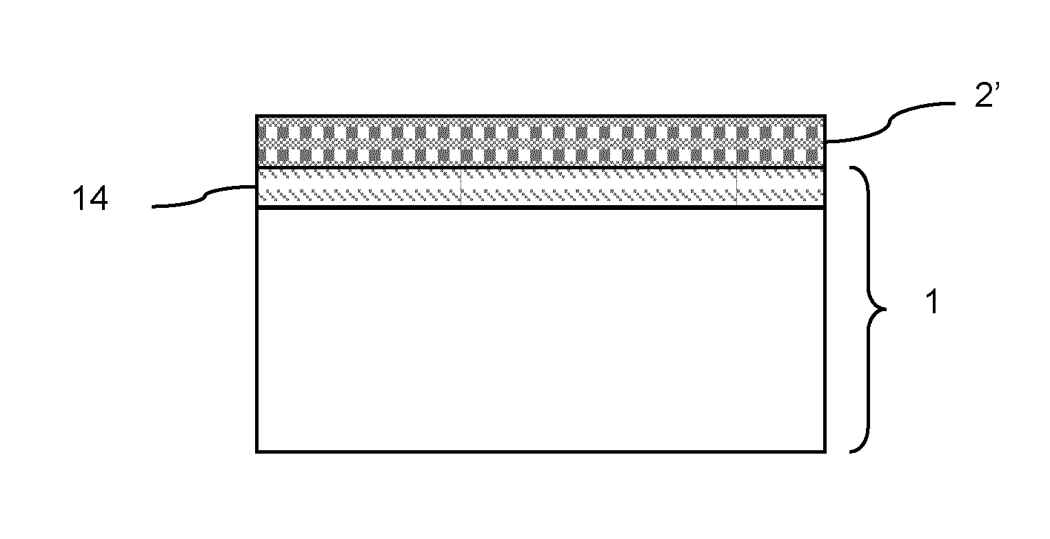
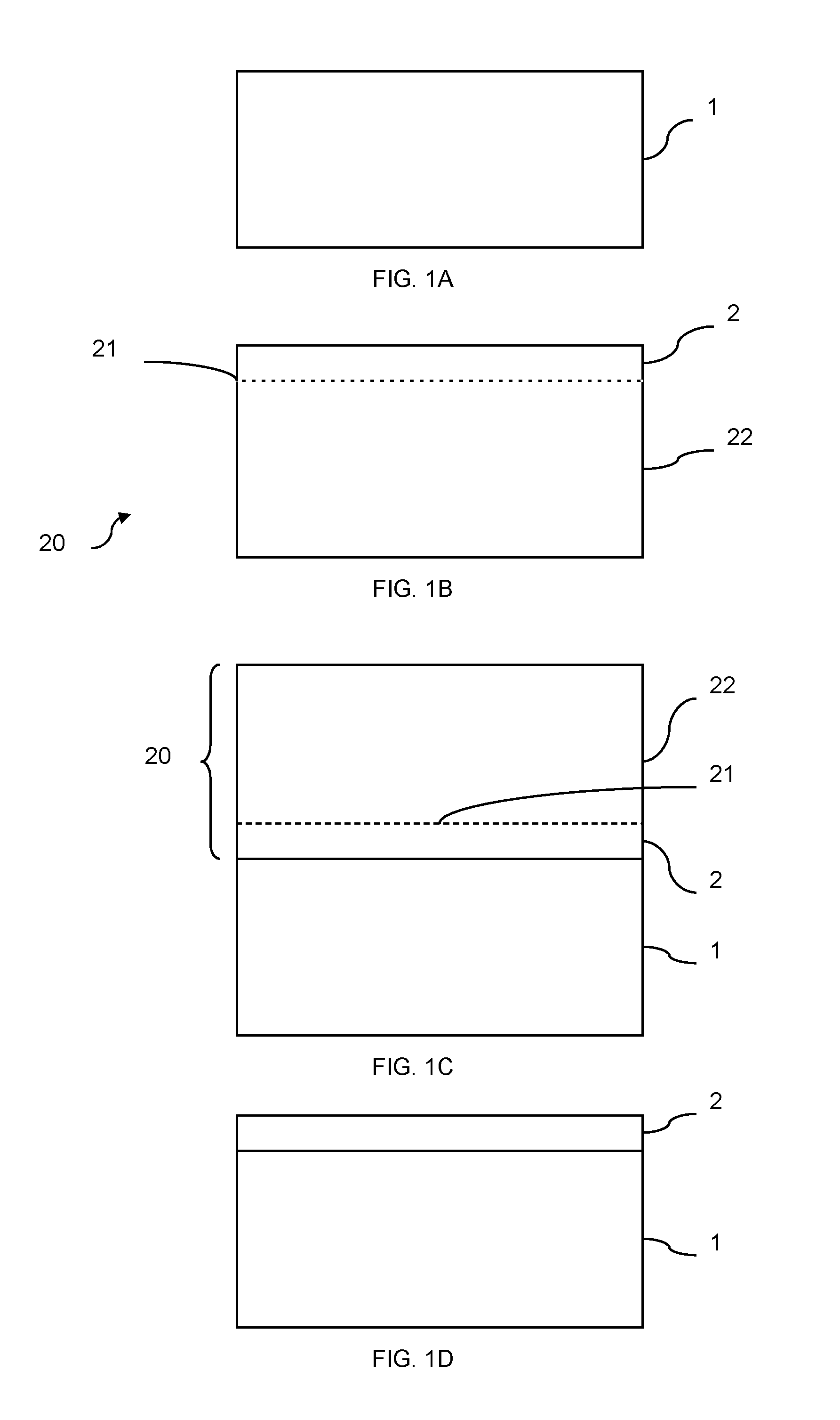
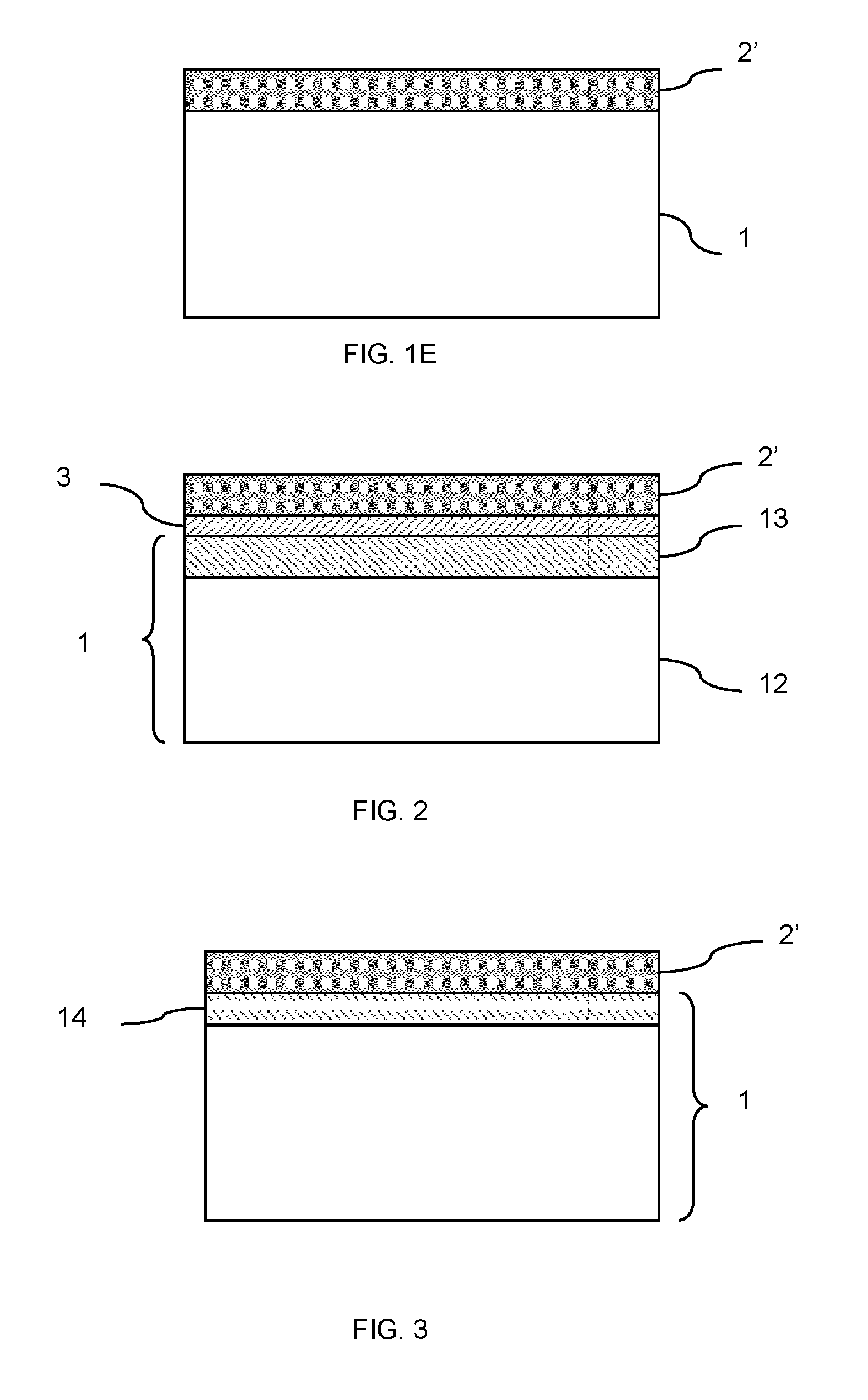
[0056]The device may be manufactured according to two main processes, described hereinafter with reference to FIGS. 1A to 1E and 4A to 4F, respectively.

First Process: Manufacture of Components in a Semiconductor Layer on the Support Substrate

[0057]A first process generally consists of first manufacturing a structure comprising the support substrate and the thin semiconductor layer for receiving the components, and manufacturing the components in the semiconductor layer.

[0058]The techniques for manufacturing components involve high temperatures, i.e., typically greater than 1000° C.

[0059]Therefore, this means that the support substrate needs to be able to withstand such temperatures.

[0060]Moreover, the support substrate should have a thermal expansion coefficient at the temperature in question, which is of the same order as that of the material of the semiconductor layer supporting the components, to prevent stress generation in the structure during the manufacture thereof.

[0061]In t...


PUM


Abstract

The invention relates to an electronic device for radio frequency or power applications, comprising a semiconductor layer supporting electronic components on a support substrate, wherein the support substrate comprises a base layer having a thermal conductivity of at least 30 W / m K and a superficial layer having a thickness of at least 5 μm, the superficial layer having an electrical resistivity of at least 3000 Ohm·cm and a thermal conductivity of at least 30 W / m K. The invention also relates to two processes for manufacturing such a device.

Description

CROSS-REFERENCE TO RELATED APPLICATIONS[0001]This application is a national phase entry under 35 U.S.C. §371 of International Patent Application PCT / EP2011 / 070220, filed Nov. 16, 2011, designating the United States of America and published in English as International Patent Publication WO 2012 / 066021 A1 on May 24, 2012, which claims the benefit under Article 8 of the Patent Cooperation Treaty and under 35 U.S.C. §119(e) to French Patent Application Serial No. 1059539, filed Nov. 19, 2010, the disclosure of each of which is hereby incorporated herein by this reference in its entirety.TECHNICAL FIELD[0002]The present invention relates to an electronic device for radiofrequency or power applications, comprising a semiconductor layer supporting electronic components on a support substrate, and processes for manufacturing such a device.BACKGROUND[0003]The production of microelectronic devices, particularly for applications in the field of radiofrequency or power, requires the placing of ...

Claims


Application Information

Patent Timeline
Patent Type & Authority Applications(United States)
IPC IPC(8): H05K1/18H01L21/762
CPCH01L21/76254H05K1/18H01L21/76251H01L21/762H01L21/20
Inventor LANDRU, DIDIERCAPELLO, LUCIANADESBONNET, ERICFIGUET, CHRISTOPHEKONONCHUK, OLEG
Owner SOITEC SA
Why Eureka
Try Eureka