Gallium nitride material transistors and methods associated with the same

a technology of gallium nitride and transistor, which is applied in the manufacture of semiconductor/solid-state devices, semiconductor devices, electrical apparatus, etc., can solve the problems of difficult to grow high-quality gallium nitride materials on certain substrates, difficult to form gallium nitride material devices meeting the property requirements of certain applications, and the application of rf power transistors may have particularly demanding property requirements

Active Publication Date: 2006-11-14
MACOM TECH SOLUTIONS HLDG INC
View PDF77 Cites 56 Cited by
  • Summary
  • Abstract
  • Description
  • Claims
  • Application Information

AI Technical Summary

Problems solved by technology

Despite the attractive properties noted above, a number of challenges exist in connection with developing gallium nitride material-based devices.
For example, it may be difficult to grow high quality gallium nitride materials on certain substrates, particularly silicon, due to property differences (e.g., lattice constant and thermal expansion coefficient) between the gallium nitride material and the substrate material.
Also, it is has been challenging to form gallium nitride material devices meeting the property requirements for certain applications.
Applications for RF power transistors may have particularly demanding property requirements.

Method used


Image

  • Gallium nitride material transistors and methods associated with the same
  • Gallium nitride material transistors and methods associated with the same
  • Gallium nitride material transistors and methods associated with the same

Examples


example 1

[0106]The following example illustrates the characterization of the performance of a gallium nitride transistor of the present invention.

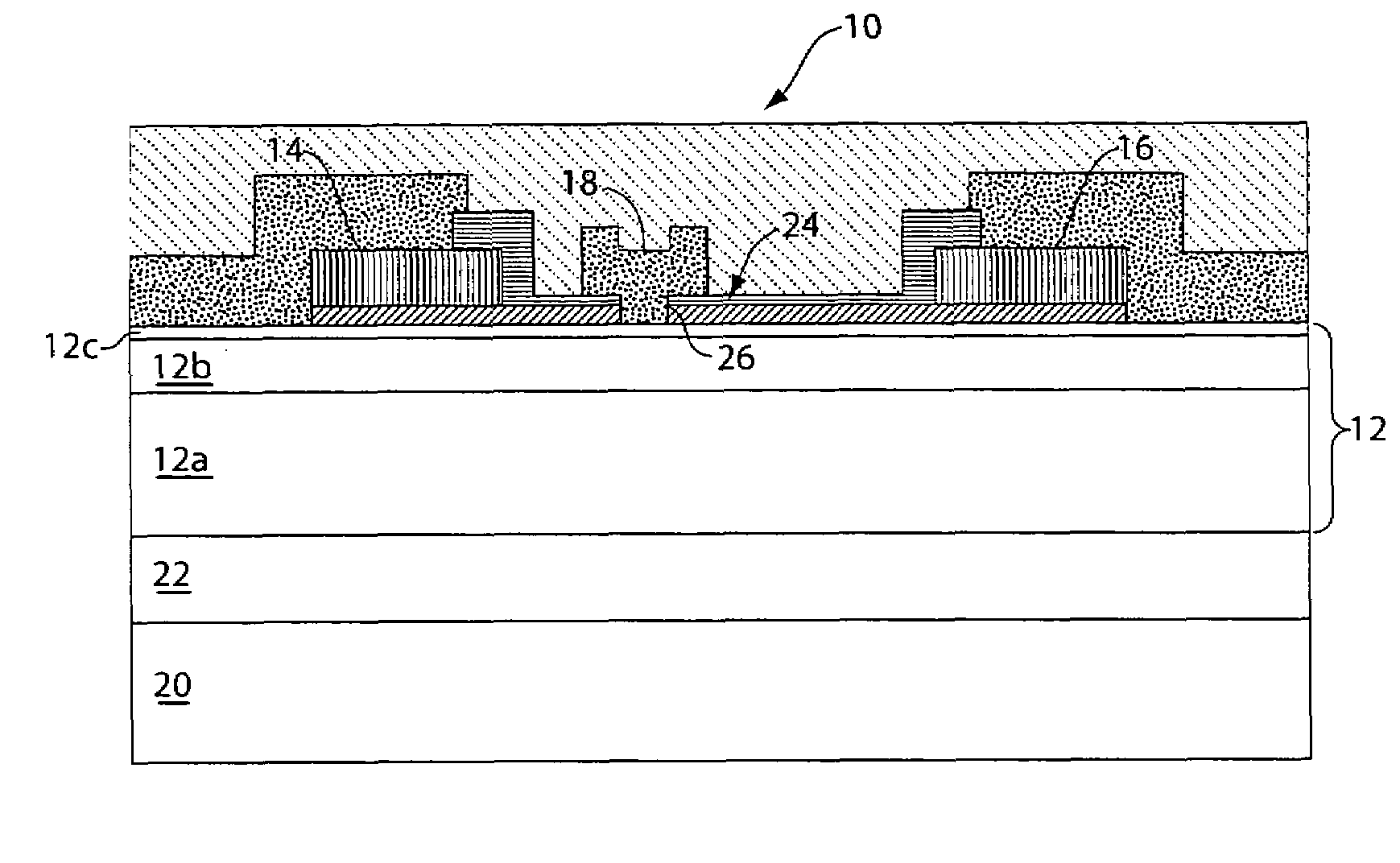
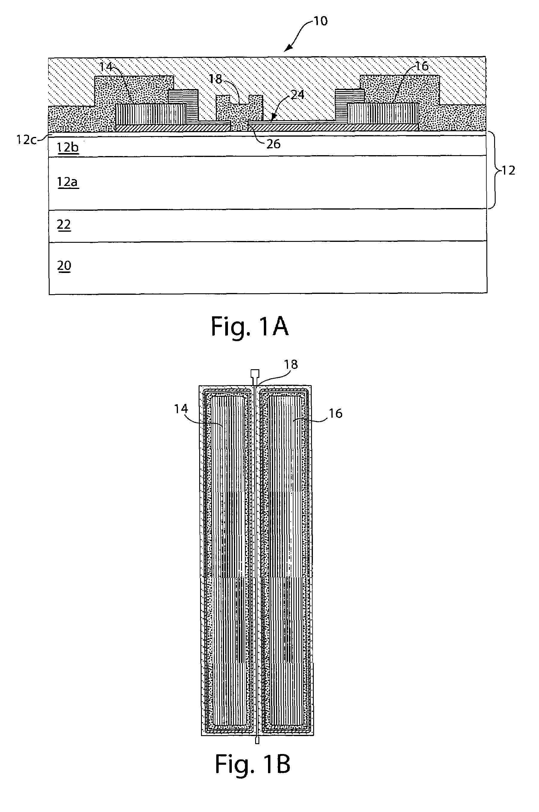
[0107]A transistor similar to the transistor illustrated in FIG. 3 was manufactured. The transistor comprised transistor building block structures similar to the structure illustrated in FIG. 1A. The transistor was mounted to a package similar to the packaged transistor shown in FIG. 4 and included a similar matching network as described above with inductor 1 being 103 picoHenry; inductor 2 being 150 picoHenry, inductor 3 being 300 picoHenry, inductor 4 being 270 picoHenry, inductor 5 being 290 picoHenry, capacitor 1 being 30 picoFarad, capacitor 2 being 25 picoFarad and capacitor 3 being 125 picoFarad.

[0108]The transistor was operated under two bias conditions within class AB operation: 1000 mA (e.g., 53% of input signal) and 25000 mA (e.g., 57% of input signal) At each operating condition, the ACPR, drain efficiency and output power were measured...

example 2

[0111]The following example illustrates the characterization of the performance of a gallium nitride transistor of the present invention.

[0112]A transistor similar to the transistor illustrated in FIG. 3 was manufactured. The transistor comprised transistor building block structures similar to the structure illustrated in FIG. 1A. The transistor was mounted to a package similar to the packaged transistor shown in FIG. 4. The performance of the transistor, as described in connection with Example 1, was evaluated in connection with two matching networks. Both matching networks have a design similar to that shown in FIG. 4. The first matching network included components having the following values: inductor 1 being 103 picohenry; inductor 2 being 150 picoHenry, inductor 3 being 300 picoHenry, inductor 4 being 270 picoHenry, inductor 5 being 290 picoHenry, capacitor 1 being 30 picoFarad, capacitor 2 being 30 picoFarad and capacitor 3 being 125 picoFarad. The second matching network was ...

example 3

[0116]The following example illustrates the characterization of the performance of a gallium nitride transistor of the present invention.

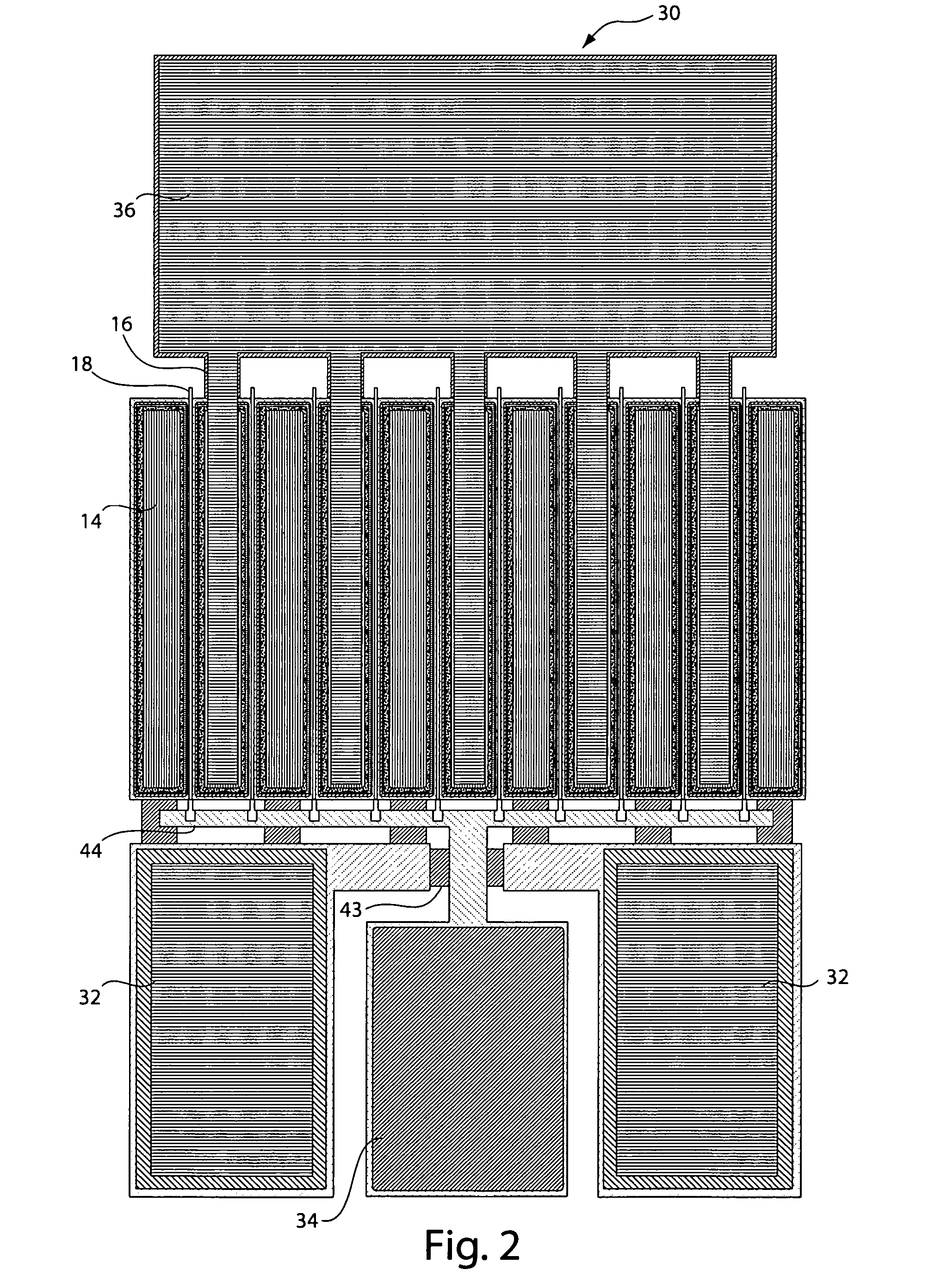
[0117]A transistor similar having 8 unit cells was manufactured. The transistor comprised transistor building block structures similar to the structure illustrated in FIG. 1A. The transistor was mounted to a simple package and matching network.

[0118]The performance of the transistor was measured. FIGS. 8A and 8B show the results. All data is reported on packaged devices with 16 mm total gate periphery measured at Vds=28 V and 2.14 GHz.

[0119]FIG. 8A shows a single-tone power-sweep reaching 30 W of saturated output power, 10 dB gain and 43% peak drain efficiency.

[0120]FIG. 8B shows efficiency and ACPR as a function of output power. The power at −39 dBc is 4.5 W (280 mW / mm) with a corresponding drain efficiency of 22.5%.

[0121]The results establish that transistors of the invention can operate at low ACPR values, as well as high efficiencies and power ...


PUM


Abstract

Gallium nitride material transistors and methods associated with the same are provided. The transistors may be used in power applications by amplifying an input signal to produce an output signal having increased power. The transistors may be designed to transmit the majority of the output signal within a specific transmission channel (defined in terms of frequency), while minimizing transmission in adjacent channels. This ability gives the transistors excellent linearity which results in high signal quality and limits errors in transmitted data. The transistors may be designed to achieve low ACPR values (a measure of excellent linearity), while still operating at high drain efficiencies and / or high output powers. Such properties enable the transistors to be used in RF power applications including third generation (3G) power applications based on W-CDMA modulation.

Description

RELATED APPLICATIONS[0001]This application claims priority to U.S. Provisional Patent Application Ser. No. 60 / 493,039, entitled “Gallium Nitride Transistor Structures and Methods”, filed Aug. 5, 2003, which is incorporated herein by reference.FIELD OF INVENTION[0002]The invention relates generally to gallium nitride material devices and, more particularly, to gallium nitride material transistors and methods associated with the same.BACKGROUND OF INVENTION[0003]Gallium nitride materials include gallium nitride (GaN) and its alloys such as aluminum gallium nitride (AlGaN), indium gallium nitride (InGaN), and aluminum indium gallium nitride (AlInGaN). These materials are semiconductor compounds that have a relatively wide, direct bandgap which permits highly energetic electronic transitions to occur. Gallium nitride materials have a number of attractive properties including high electron mobility, the ability to efficiently emit blue light, and the ability to transmit signals at high f...

Claims


Application Information

Patent Timeline
Patent Type & Authority Patents(United States)
IPC IPC(8): H01L31/072H01L29/15H01L29/20H01L29/778H01L29/812
CPCH01L29/7787H01L29/812H01L29/2003
Inventor NAGY, WALTER H.BORGES, RICARDO M.BROWN, JEFFREY D.CHAUDHARI, APURVA D.COOK, JR., JAMES W.HANSON, ALLEN W.JOHNSON, JERRY W.LINTHICUM, KEVIN J.PINER, EDWIN L.RAJAGOPAL, PRADEEPROBERTS, JOHN C.SINGHAL, SAMEERTHERRIEN, ROBERT J.VESCAN, ANDREI
Owner MACOM TECH SOLUTIONS HLDG INC
Why Eureka
Try Eureka