

Luminescence Conversion Element, Method for the Manufacture Thereof and Optoelectronic Component Having a Luminescence Conversion Element
- Summary
- Abstract
- Description
- Claims
- Application Information
AI Technical Summary
Benefits of technology
Problems solved by technology
Method used
Image

Examples
Embodiment Construction
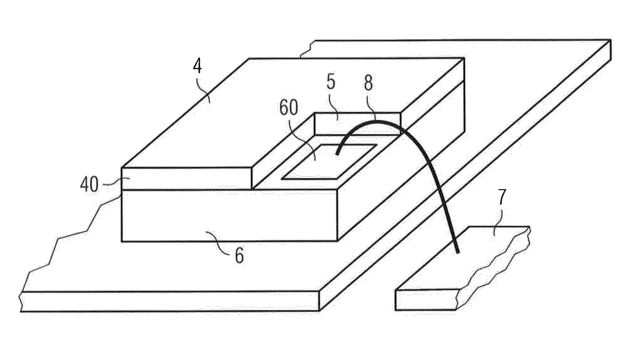
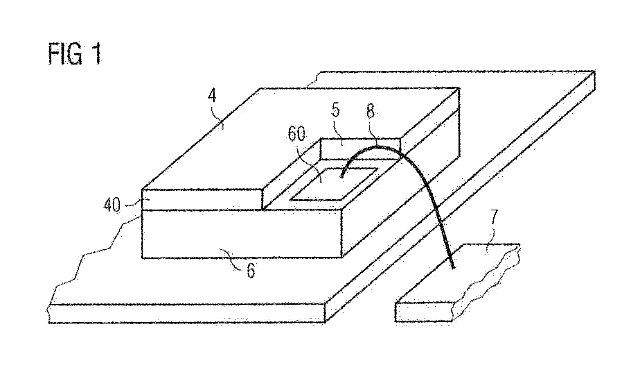
[0057]The optoelectronic component in accordance with FIG. 1 has a leadframe 7. A radiation-emitting semiconductor chip 6 is fixed on a first partial region of the leadframe 7. An L-shaped luminescence conversion element 4 in the form of a plate is arranged on said radiation-emitting semiconductor chip 6. The luminescence conversion element 4 can be adhesively bonded, for example, on to the semiconductor chip 6; for the sake of simplicity, however, the illustration of an adhesive layer has been omitted. Between that main surface of the luminescence conversion element 4 which faces the semiconductor chip 6 and the upwardly facing main surface of the luminescence conversion element 4 that faces the observer of the generated radiation, the side face 40 of the luminescence conversion element 4 can be discerned here. The luminescence conversion element 4 has a cutout 5 revealing the exposed side of the semiconductor chip 6 facing the luminescence conversion element 4. This exposed corner...
PUM
| Property | Measurement | Unit |
|---|---|---|
| Thickness | aaaaa | aaaaa |
| Distance | aaaaa | aaaaa |
| Luminescence | aaaaa | aaaaa |
Abstract
Description
Claims
Application Information