Semiconductor device and manufacturing method

a technology applied in the field of semiconductor devices and manufacturing methods, can solve the problems of mos devices manufactured by the current method having stability problems, process nodes decreasing gradually, and gate critical dimensions (cd) also decreasing continuously

Active Publication Date: 2013-11-14
SEMICON MFG INT (SHANGHAI) CORP
View PDF0 Cites 14 Cited by
  • Summary
  • Abstract
  • Description
  • Claims
  • Application Information

AI Technical Summary

Problems solved by technology

However, with the development of the semiconductor process technology, the process node decreases gradually, and the gate critical ...

Method used


Image

  • Semiconductor device and manufacturing method
  • Semiconductor device and manufacturing method
  • Semiconductor device and manufacturing method

Examples


Embodiment Construction

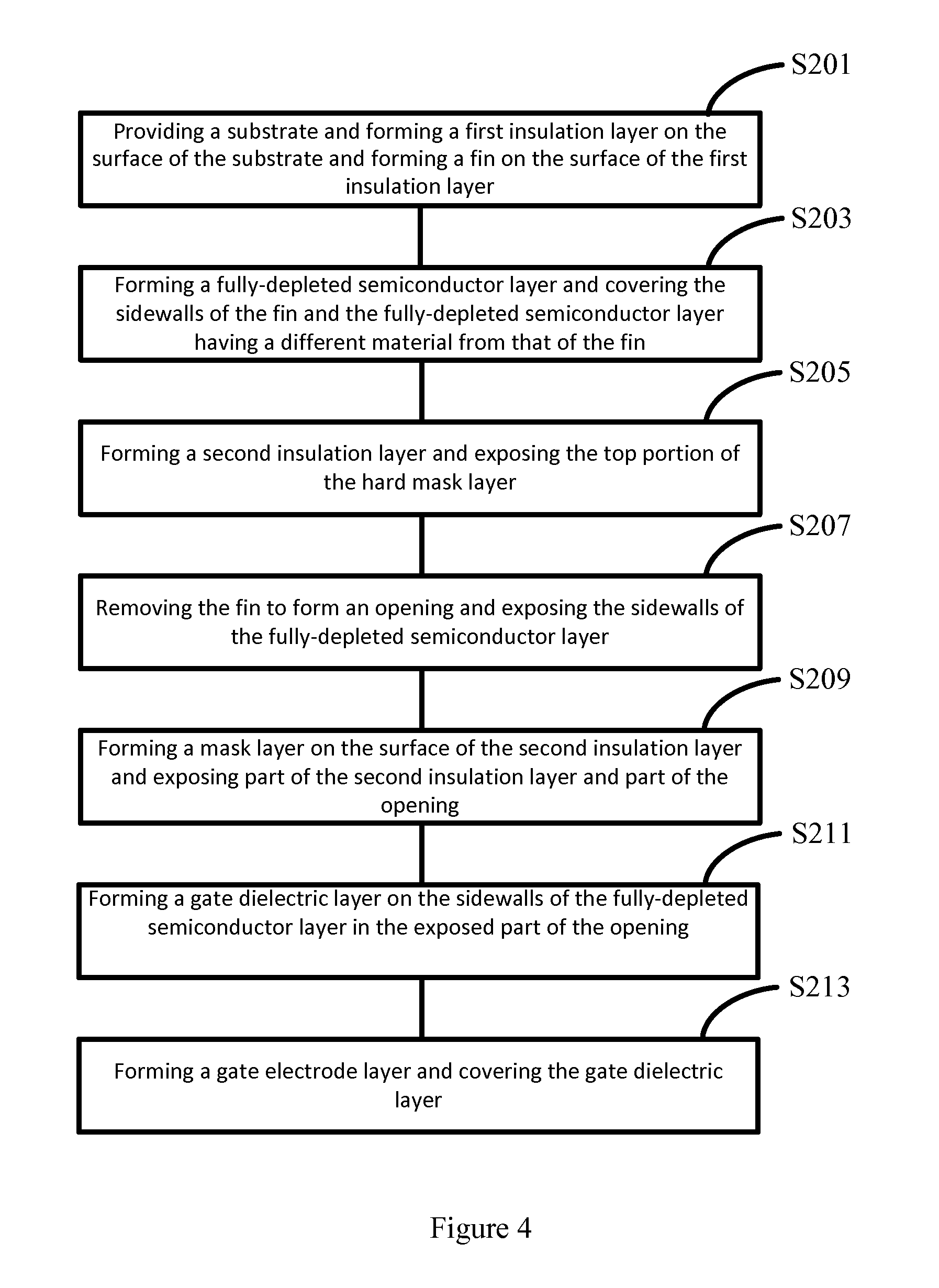
[0014]Reference will now be made in detail to exemplary embodiments of the invention, which are illustrated in the accompanying drawings. Wherever possible, the same reference numbers will be used throughout the drawings to refer to the same or like parts.

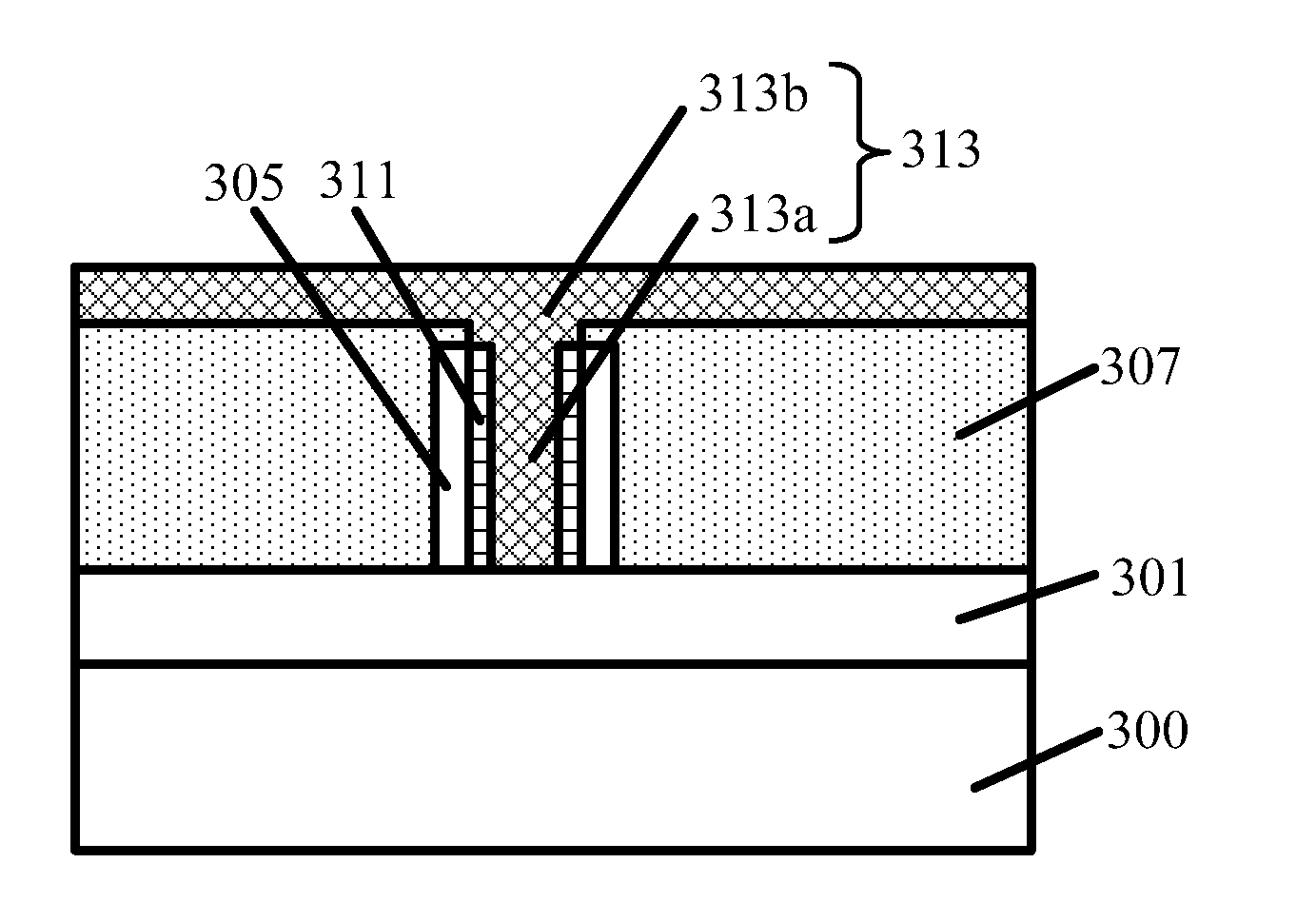
[0015]The stability issues of the semiconductor devices caused by continuous reduction on the gate critical dimensions (CD) may be solved by a variety ways. One way is to eliminate the interactions between PN junctions and between the devices.

[0016]For example, a silicon-on-insulator (SOI) may be used as a substrate for the semiconductor devices to effectively eliminate the interactions between the devices. Specifically, on the basis of the thickness of the silicon film, SOI structures may be divided into a thin-film fully-depleted SOI (FDSOI) structure and a thick-film partially-depleted SOI (PDSOI) structure. An FDSOI structure can have a lower electric field and good short-channel characteristic, thus can more effectively elimin...


PUM


Abstract

A fabrication process of a semiconductor device is disclosed. The method includes providing a semiconductor substrate with a first insulation layer formed on the semiconductor substrate and a fin formed on the surface of the first insulation layer, and forming a fully-depleted semiconductor layer on sidewalls of the fin, and the fully-depleted semiconductor layer having a material different from that of the fin. The method also includes forming a second insulation layer covering the fully-depleted semiconductor layer, and removing the fin to form an opening exposing sidewalls of the fully-depleted semiconductor layer. Further, the method includes forming a gate dielectric layer on part of the sidewalls of the fully-depleted semiconductor layer such that the part of the sidewalls of the fully-depleted semiconductor layer form channel regions of the semiconductor device, and forming a gate electrode layer covering the gate dielectric layer.

Description

CROSS-REFERENCES TO RELATED APPLICATIONS[0001]This application claims the priority of Chinese patent application no. 201210149373.6, filed on May 14, 2012, the entire contents of which are incorporated herein by reference.FIELD OF THE INVENTION[0002]The present invention generally relates to semiconductor technologies and, more particularly, to semiconductor devices and manufacturing methods.BACKGROUND[0003]There are various existing methods to manufacture metal-oxide-semiconductor (MOS) devices. For example, as shown in FIG. 1, a current method to form a MOS device includes: providing a semiconductor substrate 100; covering the surface of the semiconductor substrate 100 with an insulation layer 101; covering the surface of the insulation layer with a polycrystalline silicon layer 103; covering the surface of the polycrystalline silicon layer 103 with a photoresist layer 105.[0004]Further, as shown in FIG. 2, the current method includes: etching the polycrystalline silicon layer 103...

Claims


Application Information

Patent Timeline
IPC IPC(8): H01L29/78H01L21/36
CPCH01L29/78H01L21/36H01L29/785H01L29/0649H01L29/1033H01L29/16H01L29/1608H01L29/161H01L29/20H01L29/495H01L29/4966H01L29/51H01L29/517H01L29/518H01L29/66545H01L29/66795
Inventor HONG, ZHONGSHAN
Owner SEMICON MFG INT (SHANGHAI) CORP
Why Eureka
Try Eureka