
Scanning electron microscope

a scanning electron microscope and electron microscope technology, applied in the field of scanning electron microscope, can solve problems such as difficulty in observing the bottom of the hol

Active Publication Date: 2013-11-21
HITACHI HIGH-TECH CORP
View PDF8 Cites 20 Cited by
  • Summary
  • Abstract
  • Description
  • Claims
  • Application Information

AI Technical Summary

Benefits of technology

This patent describes a way to prevent a potential electric charge on a surface from affecting the observation, inspection, or measurement of the area using an electron beam. It does not require changing the lens conditions or other parts of the electron microscope. This technique can help to improve the accuracy and precision of electron beam based instruments.

Problems solved by technology

However, in case of the hole having the high aspect ratio, there is a case where the secondary electrons released from the bottom collide with the side wall of the hole and cannot escape from the hole, so that it is difficult to observe the bottom of the hole.

Method used


Image

  • Scanning electron microscope
  • Scanning electron microscope
  • Scanning electron microscope

Examples


embodiment 1

[0081]In order to attach the charge to the sample uniformly, scanning is made so that the charge density per unit area of the inside area within the scanned area of the electron beam is lower than that of the outside area within the scanned area. As an example of such a scanning method, there is a scanning method as illustrated in FIGS. 4A, 4B and 4C.

[0082]When the primary beam is scanned on the sample so that a square is drawn on the sample as shown in FIG. 4A, an irradiation area in the form of a square frame can be formed. In the embodiment, an example in which such a scanning method is applied to preliminary scanning of the sample is described. FIG. 4A illustrates the scanning order that scanning is made from the outside to the inside of the scanned area in order as shown by (1) to (7), although scanning may be made from the inside to the outside of the scanned area in order. Further, the faster the scanning speed is, the less the number of irradiation electrons (hereinafter ref...

embodiment 2

[0088]In the pre-dose based on the scanning method illustrated in the embodiment 1, when the area of the center part A of FIG. 5A is reduced to zero, a square irradiation area can be formed as shown in FIG. 6A. In the embodiment, scanning is continued from the outside to the inside and the scanning signal is controlled so that the scanning speed is made faster as the center part A is approached. In this case, since the charge amount per unit area is gradually reduced from the outside to the inside, the charge distribution in which the charge density in the center part A is low and the charge density in the surrounding part B is high can be formed as shown in FIG. 6B. As a result, when the electric charge accumulated in the sample by the time observation is started after pre-dose does not spread excessively, substantially uniform potential distribution can be formed in the center part A and the deviation in the field of view upon observation can be prevented as shown in FIG. 3D.

embodiment 3

[0089]As a combination of the scanning methods of FIGS. 5A and 6A, the pre-dose method in which the scanning speed is made faster as the center part A of FIG. 5A is approached and inversely the scanning speed is made slower as the outer part C is approached is also applicable. In this case, it is preferable that an adjustment apparatus which can adjust the sizes of areas A and B freely is provided so that the sizes can be adjusted in accordance with a kind of the sample or optical conditions of the electron microscope. In this method, the charge density in the center part A is zero and the density in the surrounding part B is slowly increased from the area A to the area C, so that the potential distribution can be uniformed. As a result, the horizontal shift of the primary beam in observation can be prevented and deviation in the field of view in observation can be prevented.


PUM


Abstract

The present invention has an object to provide a scanning electron microscope which suppresses a potential gradient produced by preliminary charge without changing lens conditions of an electron microscope. As an aspect to achieve the above object, there is proposed a scanning electron microscope in which a scanning deflector is controlled so that a second beam is scanned to detect electrons released from a sample after scanning a first beam on the sample to charge the surface of the sample and the first beam is scanned so that charge density in a surrounding part within a scanned area by the first beam is increased relatively as compared with a center part within the scanned area by the first beam.

Description

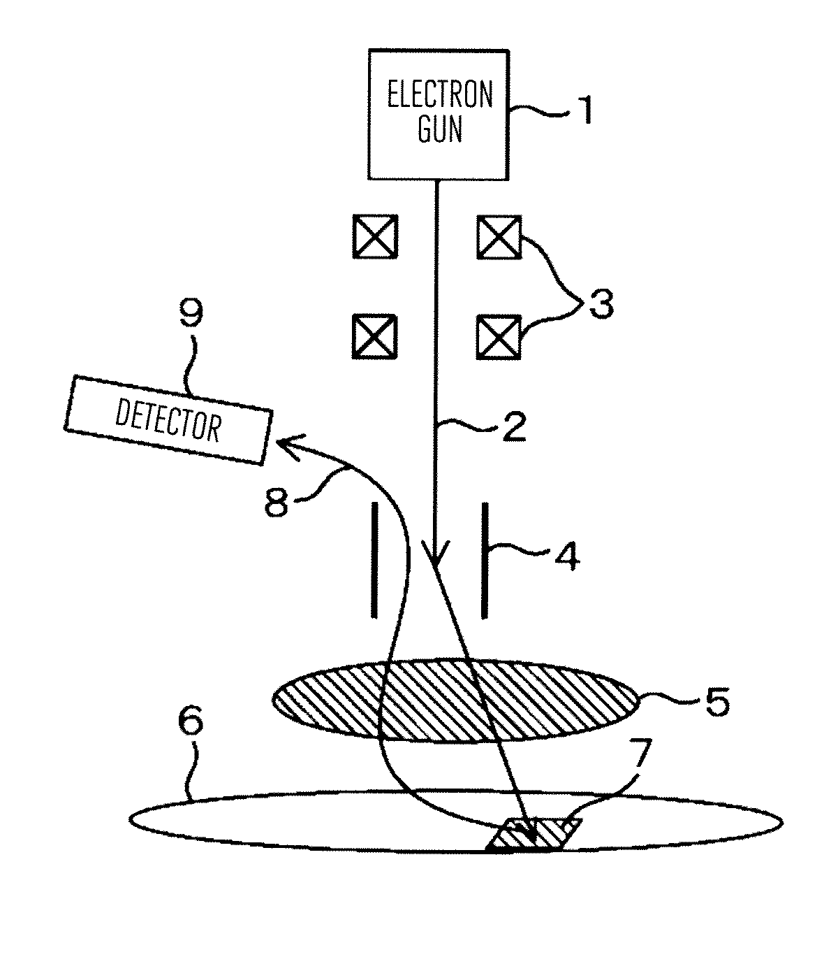
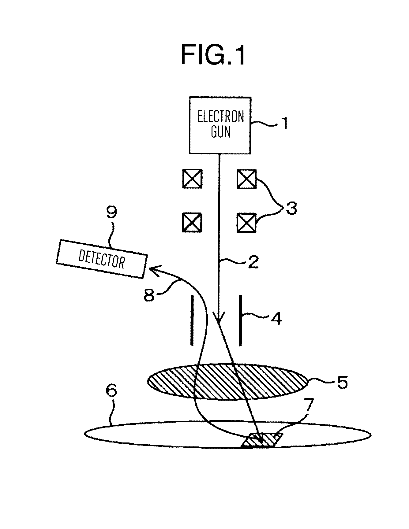
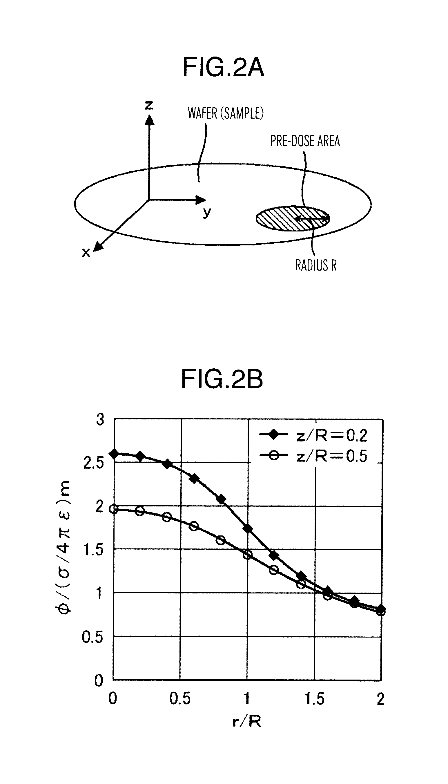
TECHNICAL FIELD[0001]The present invention relates to a scanning electron microscope and more particularly to a preliminary charge method of charging a sample by scanning of electron beam and a scanning electron microscope which attaches preliminary charge to the sample.BACKGROUND ART[0002]A scanning electron microscope (SEM) is an apparatus which detects secondary electrons (SE) and backscattered electrons (BSE) released from a sample by irradiating the sample with an electron beam (hereinafter also referred to as a primary beam). The detected signal can be converted into an image or line profile to thereby observe, inspect or measure the sample. Electron microscopes are widely applied to measurement of semiconductor devices and measurement technique thereof must be applied to measurement of various patterns with miniaturization of semiconductor devices.[0003]Recently, in particular, there is a need for observation and measurement of a hole structure having a high aspect ratio name...

Claims


Application Information

Patent Timeline
Patent Type & Authority Applications(United States)
IPC IPC(8): H01J37/28
CPCH01J37/28H01J37/1474H01J2237/004H01J2237/0048H01J2237/281
Inventor HOQUE, SHAHEDULKAWANO, HAJIME
Owner HITACHI HIGH-TECH CORP
Learn More