TFT array substrate and forming method thereof, and display panel

a technology of array substrate and substrate, applied in the field of display, can solve the problems of low k organic material used, reduced yield of manufacturing the existing tft array base plate, and high manufacturing cost, and achieve the effects of low yield, high manufacturing cost, and high aperture ratio

Active Publication Date: 2013-11-28
BEIHAI HKC OPTOELECTRONICS TECH CO LTD
View PDF8 Cites 30 Cited by
  • Summary
  • Abstract
  • Description
  • Claims
  • Application Information

AI Technical Summary

Benefits of technology

[0005]According to the present invention, a problem to be solved is the complex process, the low yield a

Problems solved by technology

However, the low K organic material used is expensive and the manufacturing process is complex.
Therefore,

Method used


Image

  • TFT array substrate and forming method thereof, and display panel
  • TFT array substrate and forming method thereof, and display panel
  • TFT array substrate and forming method thereof, and display panel

Examples


first embodiment

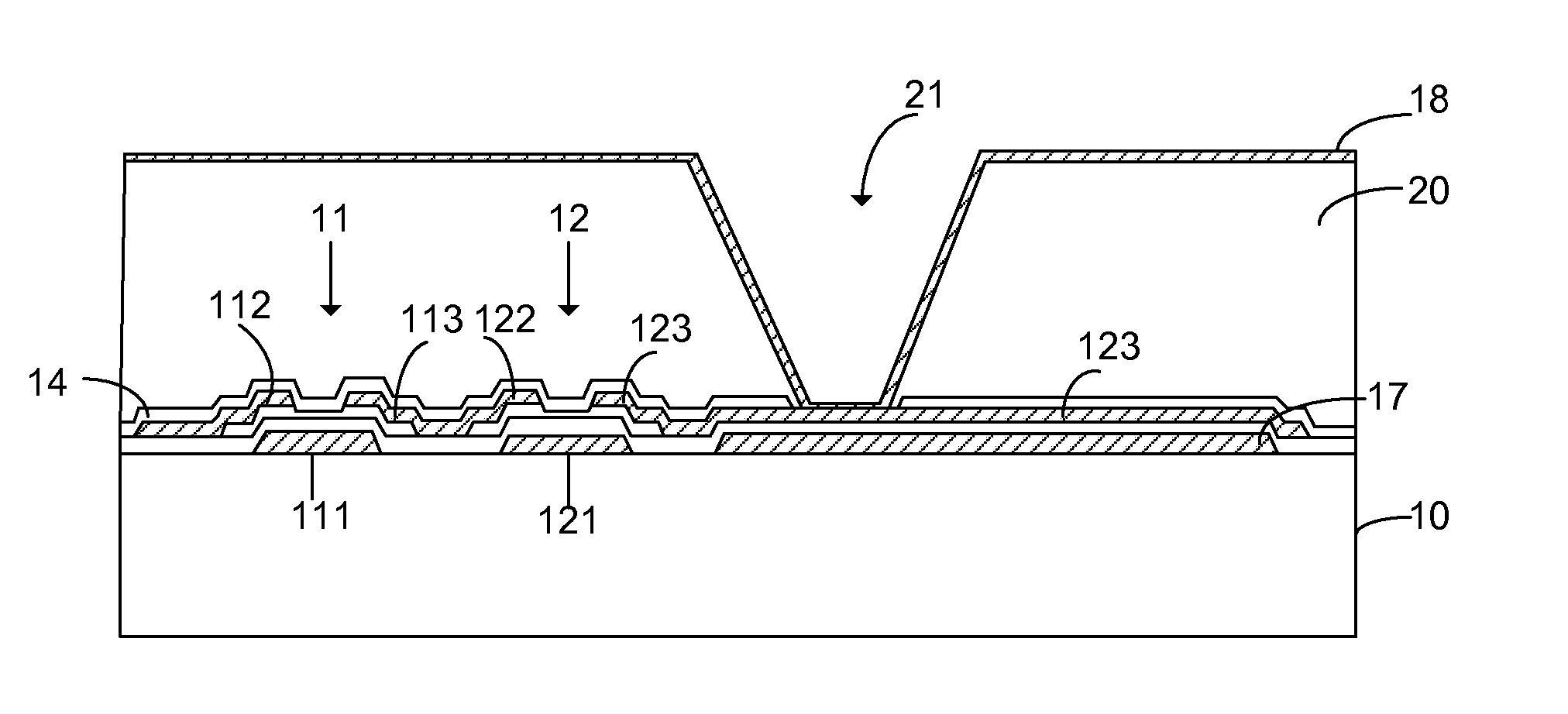
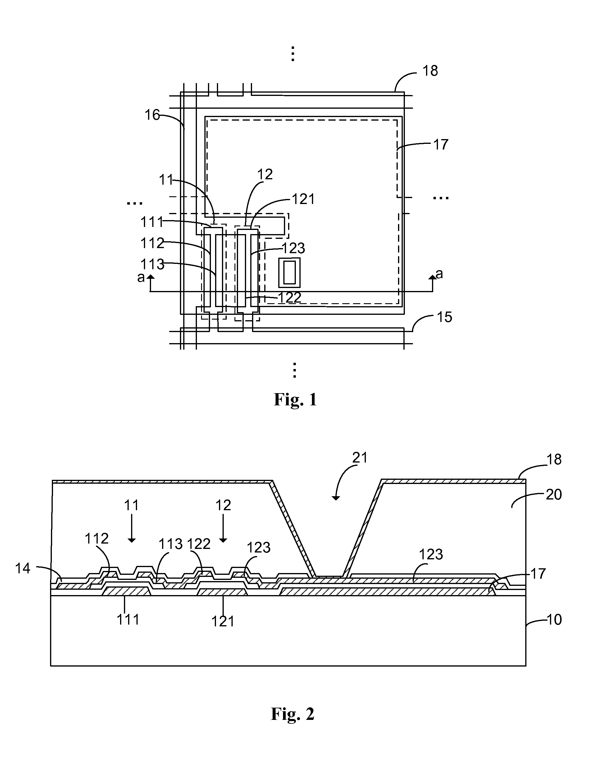
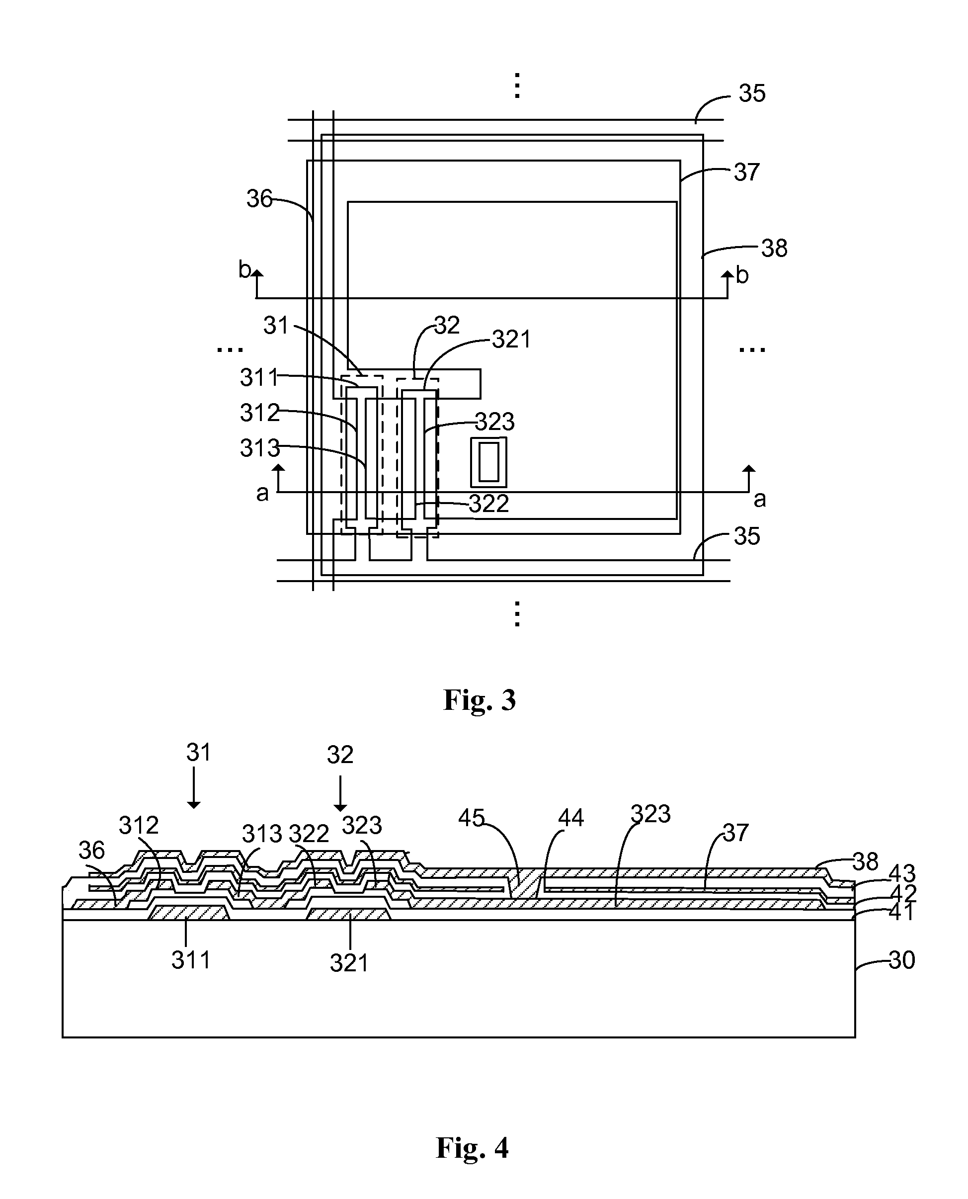
[0054]A First Embodiment

[0055]FIG. 3 is a schematic partial plan view of a TFT array substrate according to a first embodiment of the present invention, FIG. 4 is a schematic sectional view of the TFT array substrate taken along the line a-a in FIG. 3, and FIG. 5 is a schematic sectional view of the TFT array substrate taken along the line b-b in FIG. 3.

[0056]Referring to FIG. 3, FIG. 4 and FIG. 5, the TFT array substrate according to the first embodiment of the present invention includes a substrate 30. The substrate 30 is transparent and may be made of glass, quartz and the like. The first embodiment also includes an array of TFT switches is disposed on the substrate 30. The array includes multiple scan lines 35 (the multiple scan lines 35 are substantially parallel with each other), multiple data lines 36 intersecting with the multiple scan lines 35 (the multiple data lines 36 are substantially parallel with each other and intersecting with the multiple scan lines 35 perpendicula...

second embodiment

[0094]A Second Embodiment

[0095]FIG. 16 is a schematic partial plan view of a TFT array substrate according to a second embodiment of the present invention, FIG. 17 is a schematic sectional view of the TFT array substrate taken along the line a-a in FIG. 16, and FIG. 18 is a schematic plan view of pixel arrangement of the TFT array substrate according to the second embodiment of the present invention. Referring to FIG. 16, FIG. 17 and FIG. 18, the TFT array substrate according to the second embodiment of the present invention includes: a substrate 100; an array of TFT switches disposed on the substrate 100, which includes multiple scan lines 52, multiple data lines 51 intersecting with the multiple scan lines 52, and multiple TFT switches. The multiple scan lines 52 are disposed substantially parallel with each other, and the multiple data lines 51 are disposed substantially parallel with each other and substantially perpendicular to the multiple scan lines 52. In addition, the regio...


PUM


Abstract

A TFT array substrate is disclosed. The TFT array substrate includes an array of TFT switches including scan lines, data lines intersecting the scan lines, and TFT switches. Each of the TFT switches includes a gate electrode electrically connected to a scan line, a source electrode electrically connected to a data line, and a drain electrode. The TFT array substrate also includes an array of pixel electrodes, each of the pixel electrodes is electrically connected to the drain electrode of a corresponding TFT switch. At least one first pixel electrode is disposed in the array of the pixel electrodes, and each first pixel electrode has an overlapping portion overlapped by at least one of the scan lines and the data lines. In addition, in the overlapping portion, a shielding electrode layer is located between the first pixel electrode and at least one of the scan line and the data line overlapping the first pixel electrode.

Description

CROSS-REFERENCES TO RELATED APPLICATIONS[0001]This application claims priority to and is a continuation of International Patent Application PCT / CN2012 / 078234, entitled “TFT ARRAY SUBSTRATE AND FORMING METHOD THEREOF, AND DISPLAY PANEL,” filed on Jul. 5, 2012, which claims priority to Chinese patent application No. 201110383609.8, entitled “TFT ARRAY SUBSTRATE AND FORMING METHOD THEREOF, AND DISPLAY PANEL” and filed with the State Intellectual Property Office on Nov. 25, 2011, the contents of which are incorporated herein by reference in their entirety.FIELD OF THE INVENTION[0002]The present invention relates to the field of display, and in particular to a TFT array substrate, method of manufacturing the same, and a display panel.BACKGROUND OF THE INVENTION[0003]In recent years, flat panel displays represented by electronic books and liquid crystal displays are more and more popular. Most electronic books and liquid crystal displays are of the type of active matrix, which have a TFT ...

Claims


Application Information

Patent Timeline
IPC IPC(8): G02F1/1343H01L33/00G02F1/1676
CPCG02F1/1343H01L33/0041H01L29/78633H01L27/124G02F1/136227G02F1/13624G02F2201/40G02F1/136218H10K59/124H10K59/126G02F1/1676G02F1/1368
Inventor CHEN, HAOMA, JUNWU, TIANYI
Owner BEIHAI HKC OPTOELECTRONICS TECH CO LTD
Why Eureka
Try Eureka