Semiconductor process

a technology of semiconductors and processes, applied in the field of semiconductors, can solve the problems of reducing the epitaxial layer forcing stress effect and how to increase the driving current of mos transistors, and achieve the effect of reducing the epitaxial layer doped concentration and reducing the forcing stress

Active Publication Date: 2013-11-28
MARLIN SEMICON LTD
View PDF5 Cites 16 Cited by
  • Summary
  • Abstract
  • Description
  • Claims
  • Application Information

AI Technical Summary

Benefits of technology

[0007]The present invention provides a semiconductor process that forms an epitaxial structure after a source / drain is formed, so that said problems can be solved.
[0010]According to the above, the present invention provides a semiconductor process that forms an epitaxial structure after a source / drain is formed. In this way, the epitaxial structure of the present invention can skip processes with a high processing temperature, such as a source / drain annealing process or the likes. Therefore, the problems of dopants out-diffusion can be avoided, so that circuit leakage caused by electrons passing through gate channels, and the reduction of forcing stress effect caused by the decreasing doped concentration of the epitaxial layer can be avoided.

Problems solved by technology

As the semiconductor processes advance to very deep sub micron era, such as 65-nm node or beyond, how to increase the driving current of MOS transistors has become a critical issue.
However, the epitaxial layer such as the silicon germanium (SiGe) or silicon carbide (SiC) epitaxial layer will suffer thermal processes such as a source / drain annealing process or etc in semiconductor processes.
These thermal processes cause dopants of the epitaxial layer to diffuse outwards, leading to electrons passing through the gate channels which provokes circuit leakage, and accordingly reduces the forcing stress effect of the epitaxial layer.

Method used


Image

  • Semiconductor process
  • Semiconductor process
  • Semiconductor process

Examples


Embodiment Construction

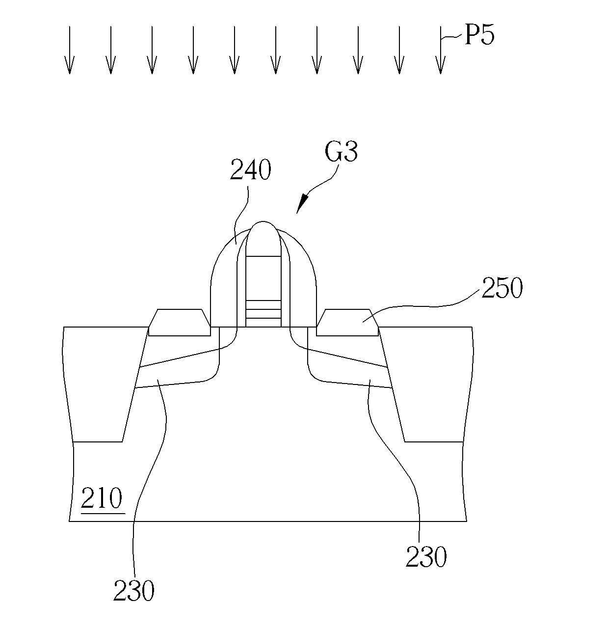
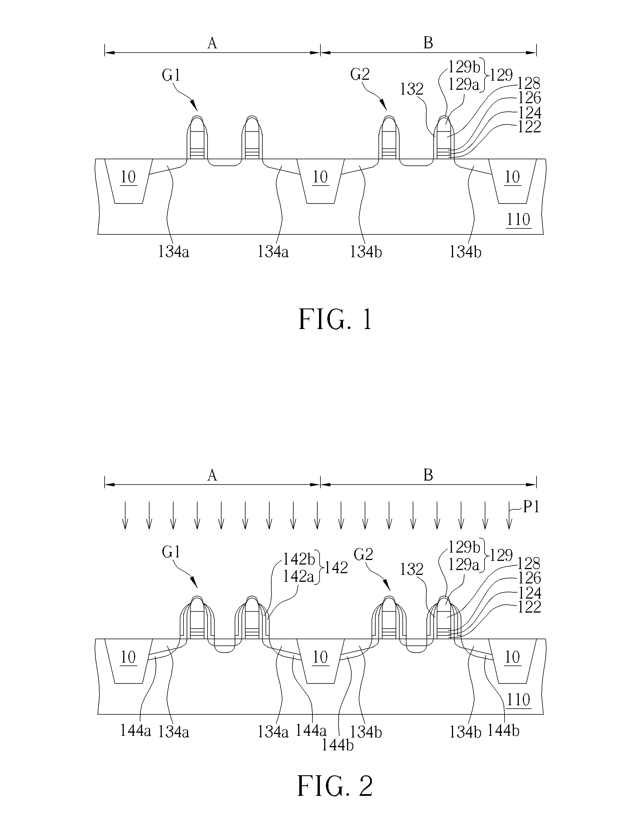
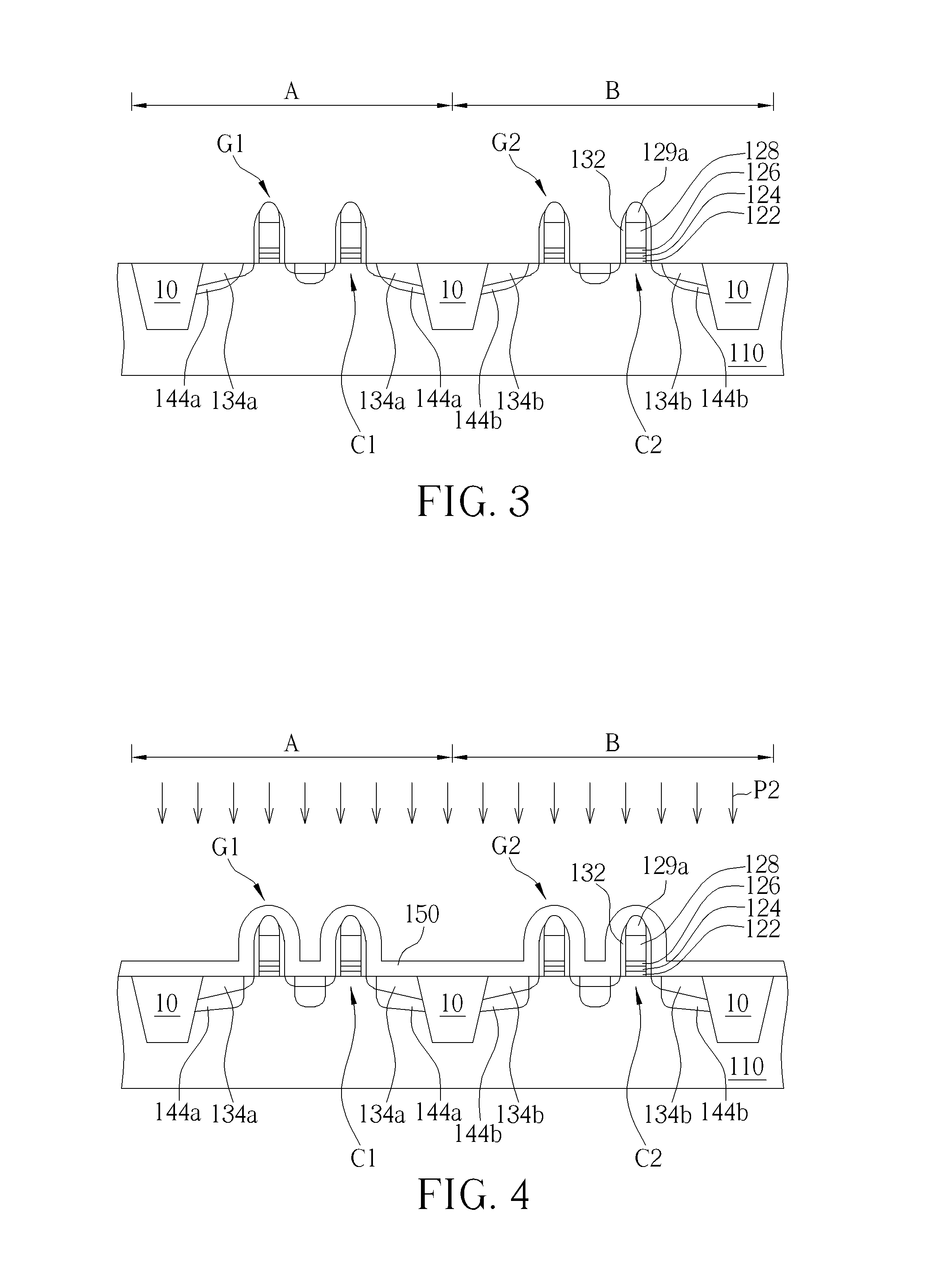
[0015]FIGS. 1-8 schematically depict cross-sectional views of a semiconductor process according to an embodiment of the present invention. As shown in FIG. 1, a substrate 110 is provided. The substrate 110 may be a semiconductor substrate such as a silicon substrate, a silicon containing substrate, a III-V group-on-silicon (such as GaN-on-silicon) substrate, a graphene-on-silicon substrate or a silicon-on-insulator (SOI) substrate. Isolation structures 10 are formed in the substrate 110. The isolation structures 10 may be shallow trench isolation (STI) structures, formed through a shallow trench isolation (STI) process, but it is not limited thereto. The details of the shallow trench isolation (STI) process are known in the art, and will therefore not be described herein. In this embodiment, the substrate 110 is divided into a first area A and a second area B by the isolation structures 10, wherein the first area A is used to form a PMOS transistor area, while the second area B is u...


PUM


Abstract

A semiconductor process includes the following steps. A gate structure is formed on a substrate. A main spacer is formed on the substrate beside the gate structure. A source / drain is formed in the substrate beside the main spacer. After the source / drain is formed, an epitaxial structure is formed in the substrate beside the main spacer. A gate structure may be respectively formed in a first area and a second area of a substrate. A main spacer is formed on the substrate respectively beside the two gate structures. A source / drain is formed in the substrate respectively beside the two spacers. After the two source / drains are formed, an epitaxial structure is formed in the substrate respectively beside the main spacers.

Description

BACKGROUND OF THE INVENTION[0001]1. Field of the Invention[0002]The present invention relates generally to a semiconductor process, and more specifically to a semiconductor process that forms an epitaxial structure after a source / drain is formed.[0003]2. Description of the Prior Art[0004]For decades, chip manufacturers have made metal-oxide-semiconductor (MOS) transistors faster by making them smaller. As the semiconductor processes advance to very deep sub micron era, such as 65-nm node or beyond, how to increase the driving current of MOS transistors has become a critical issue. In order to improve the device performances, crystal strain technology has been developed. Crystal strain technology is becoming more and more attractive as a mean for getting better performances in the field of CMOS transistor fabrication. Putting a strain on a semiconductor crystal alters the speed at which charges move through said crystal. Strain makes CMOS transistors work better by enabling electrica...

Claims


Application Information

Patent Timeline
Patent Type & Authority Applications(United States)
IPC IPC(8): H01L21/336
CPCH01L21/823425H01L21/823412H01L21/823468H01L21/823807H01L21/823814H01L21/823864
Inventor CHANG, CHUNG-FUHUNG, YU-HSIANGHUANG, SHIN-CHUANLIU, CHIA-JONGWU, YEN-LIANGCHOU, PEI-YU
Owner MARLIN SEMICON LTD
Why Eureka
Try Eureka