Eureka AIR delivers breakthrough ideas for toughest innovation challenges, trusted by R&D personnel around the world.

Method of etching of soi substrate, and back-illuminated photoelectric conversion module on soi substrate and process of manufacture thereof

a technology of photoelectric conversion module and soi substrate, which is applied in the direction of electrical equipment, semiconductor devices, radio frequency control devices, etc., can solve the problems of increasing cost, reducing production efficiency, and reducing the area of light receiving surface beyond

Active Publication Date: 2013-12-05
TOHOKU UNIV
View PDF5 Cites 6 Cited by
  • Summary
  • Abstract
  • Description
  • Claims
  • Application Information

AI Technical Summary

Benefits of technology

The patent describes the etching method of the present invention and its use in the production of a backside illumination type photoelectric conversion module. The method involves exposing the free surface of a Si substrate in the SOI substrate to a specific composition of fluonitric acid to quickly and flatly perform wet etching. This allows for the efficient production of the photoelectric conversion module while also reducing absorption of entrance light and improving the flatness of the light entrance surface in backside illumination. The method also includes a steps of etching the free surface of the Si substrate of the pre-photoelectric conversion module to significantly enhance the efficiency of the production.

Problems solved by technology

However, there is a limitation in it.
Furthermore, a major cause of the area of the light receiving surface becoming smaller beyond necessity as density increases is the area occupied by wiring for feeding signals to the individual photoelectric conversion elements and the drive elements thereof and for applying a predetermined voltage to a predetermined portion of the image sensor.
In order to avoid it, it is proposed not to reduce the resistance by increasing the width of the wiring but to reduce the resistance by increasing the thickness of the wiring, and it becomes commercially practical; however, this increases the number of manufacturing steps to cause cost increase.
Hence, a large amount of time is taken to limit the efficiency of production, and thus it becomes a cause of cost increase.

Method used


Image

  • Method of etching of soi substrate, and back-illuminated photoelectric conversion module on soi substrate and process of manufacture thereof
  • Method of etching of soi substrate, and back-illuminated photoelectric conversion module on soi substrate and process of manufacture thereof
  • Method of etching of soi substrate, and back-illuminated photoelectric conversion module on soi substrate and process of manufacture thereof

Examples


Embodiment Construction

[0036]An embodiment of the present invention will be described in detail below with reference to accompanying drawings.

[0037](Etching method according to the present invention)

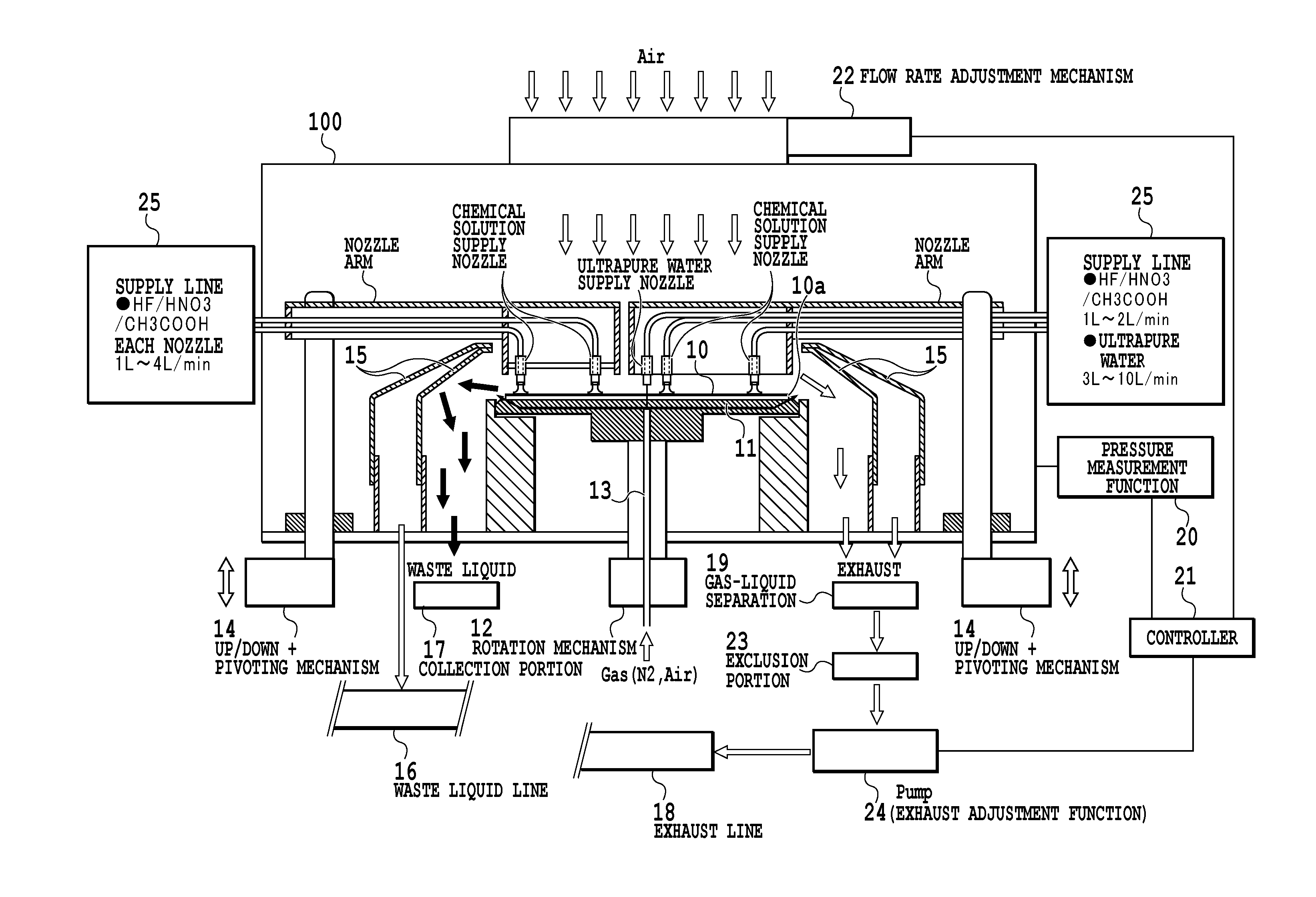
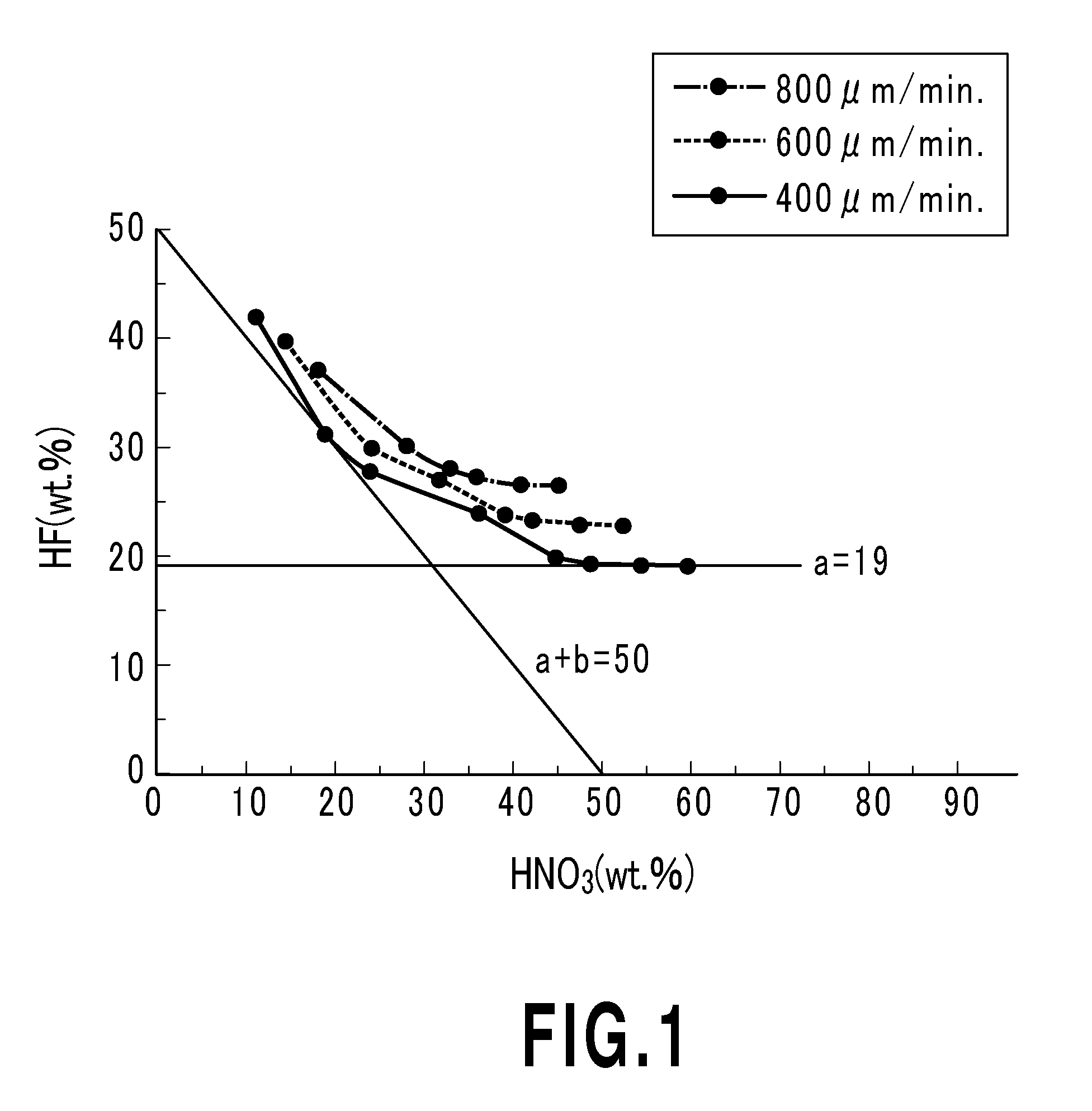
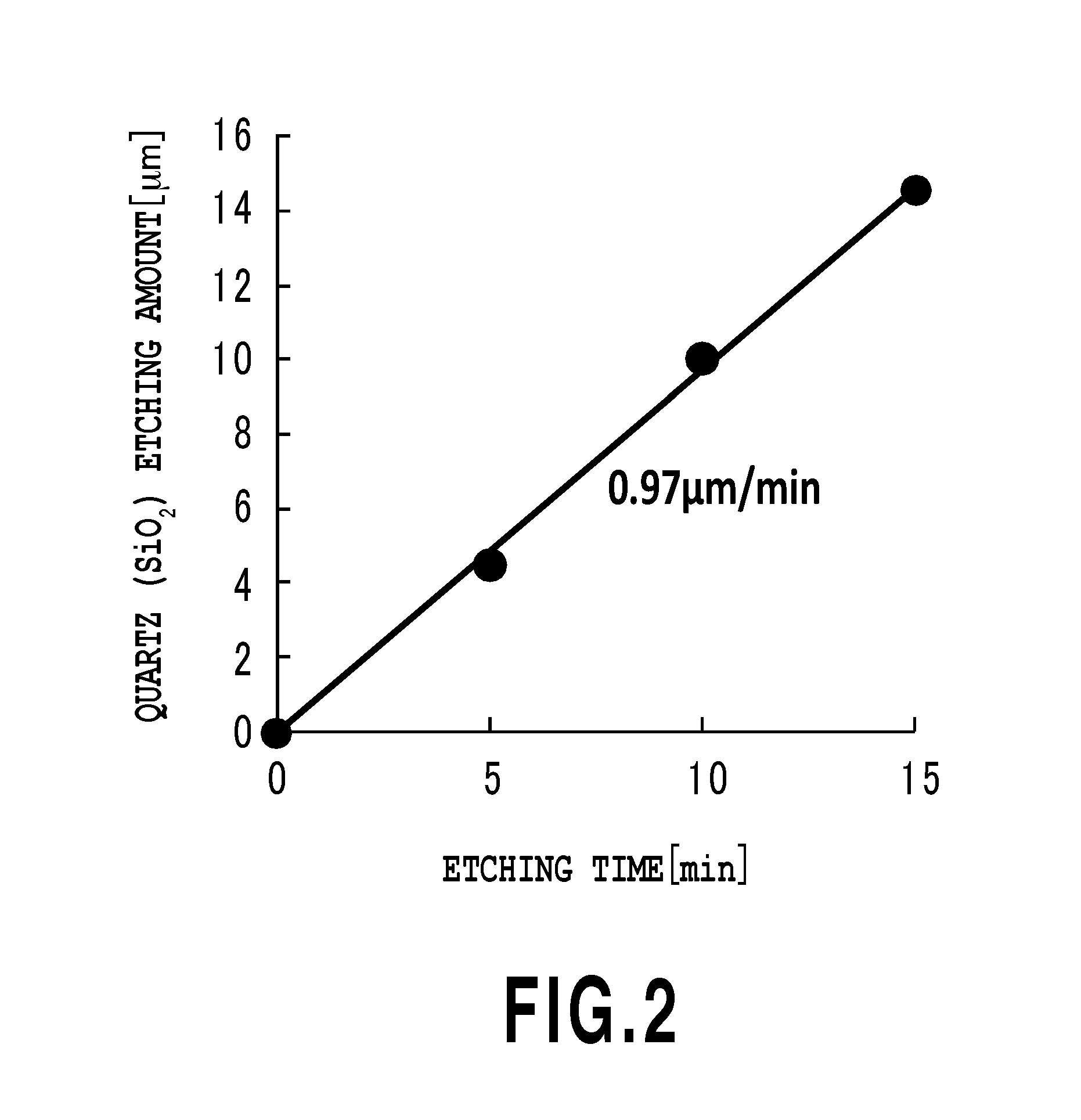
[0038]An etching method according to the present invention performs wet etching on the Si substrate of an SOI substrate with highly concentrated fluonitric acid. Fluonitric acid can be generally represented by HF(a)HNO3(b)H2O(c) (where a, b and c are values representing concentrations, the unit thereof is wt % and a+b+c=100). The present inventors find that the etching rate of an SiO2 layer with the highly concentrated fluonitric acid is significantly lowered by the appropriate selection of its composition as compared with the etching rate of the Si substrate, and etch the Si substrate until the SiO2 layer is exposed. In this way, it is possible to rapidly etch the Si substrate and significantly enhance the flatness of the etched surface as compared with a conventional method. Even when the composition of the ...


PUM


Abstract

A method of etching capable of rapidly and flatly performing wet etching on a Si substrate using fluonitric acid represented by HF(a)HNO3(b)H2O(c) (where the unit of a, b and c is wt % and a+b+c=100). The etching rate of an SiO2 layer with the highly concentrated fluonitric acid is significantly lowered by the appropriate selection of its composition as compared with the etching rate of the Si substrate, and etch the Si substrate until the SiO2 layer is exposed. In this way, it is possible to rapidly etch the Si substrate and significantly enhance the flatness of the etched surface.

Description

TECHNICAL FIELD[0001]The present invention relates to a method of etching an SOI substrate and a backside illumination type photoelectric conversion module on an SOI substrate and a method of producing it.BACKGROUND ART[0002]A semiconductor device using an SOI (Silicon On Insulator) substrate is advantageous over a semiconductor device using a Si substrate in an operation speed and energy saving, and, even in the field of a photoelectric conversion device such as an image sensor, it is proposed to utilize the SOI substrate. Here, the “SOI substrate” refers to a substrate in which an SiO2 layer is inserted between a Si substrate and a surface Si layer. The “surface Si layer” may contain an impurity.[0003]An image sensor such as a CCD image sensor or a CMOS image sensor is a sensor in which photoelectric conversion elements such as photodiodes are arranged in a matrix, and each photoelectric conversion element functions as a pixel. In recent years, the opportunity of performing shooti...

Claims


Application Information

Patent Timeline
Patent Type & Authority Applications(United States)
IPC IPC(8): H01L31/0248H01L21/306
CPCH01L31/0248H01L21/30604H01L21/6708H01L27/1464H01L29/78603H01L21/306H01L21/308H01L27/12H01L27/146
Inventor OHMIOHASHI, TOMOTSUGUYOSHIKAWA, KAZUHIROYOSHIDA, TATSUROUCHIMURA, TEPPEISOEDA, KAZUKISUGAWA, SHIGETOSHI
Owner TOHOKU UNIV
Why Eureka
Eureka Blog
Learn More