Semiconductor device

Active Publication Date: 2013-12-05
PANASONIC SEMICON SOLUTIONS CO LTD
View PDF12 Cites 6 Cited by
  • Summary
  • Abstract
  • Description
  • Claims
  • Application Information

AI Technical Summary

Benefits of technology

The present invention aims to provide a semiconductor device that can relax stress on the substrate caused by a through-silicon via, which can prevent fluctuations in the properties of transistors close to the via. This results in a highly reliable semiconductor device. The method of manufacturing the semiconductor device follows the same aim of reducing stress and preventing property fluctuations.

Problems solved by technology

However, the methods of relaxing stress described above need an additional process of forming a relaxation layer or a metal layer, and this entails problems of a limitation in performance of a material to be added and complicated process.

Method used


Image

  • Semiconductor device
  • Semiconductor device
  • Semiconductor device

Examples


first exemplary embodiment

[0045]A first exemplary embodiment of the present invention will be described below with reference to the drawings.

[0046]FIGS. 1A to 3 are sectional views illustrating a process of a method of manufacturing a semiconductor device according to a first exemplary embodiment of the present invention.

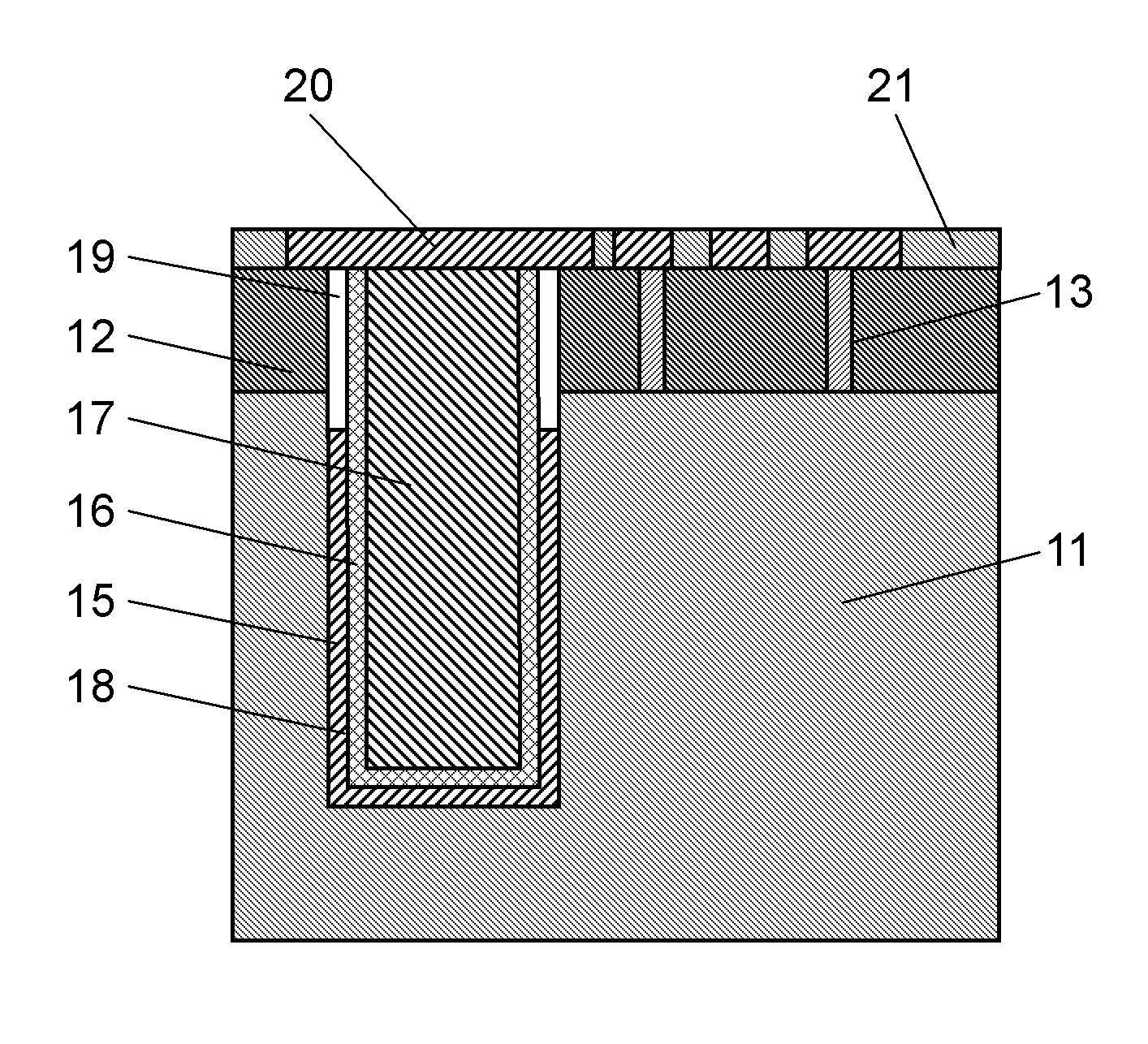
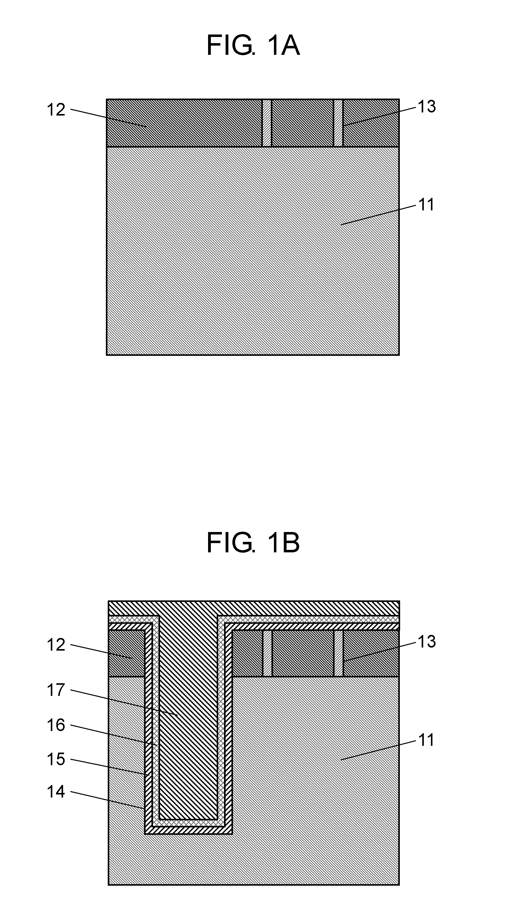
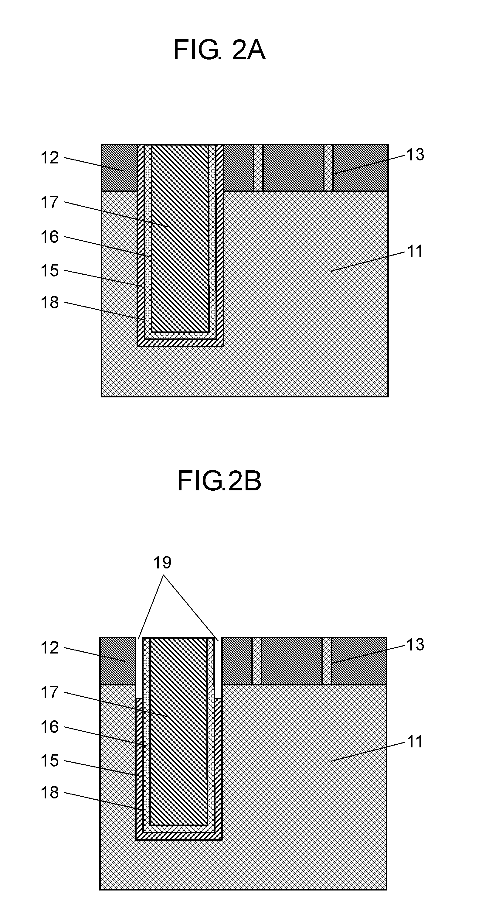
[0047]As illustrated in FIG. 1A, elements (not illustrated) such as a transistor or a resistor are formed on semiconductor substrate 11, first interlayer insulating film 12 made of a silicon oxide film and including the elements and a wiring layer is formed, and then, contact plug 13 is formed in first interlayer insulating film 12. In this case, a thickness of first interlayer insulating film 12 is 500 nm, for example.

[0048]Next, as illustrated in FIG. 1B, through-silicon via hole 14 having a diameter of 5 μm and a depth of 50 μm is formed by using a lithography technique and a dry etching technique, and then, insulating film 15 made of a silicon nitride film having a thickness of 200 nm is...

second exemplary embodiment

[0057]A second exemplary embodiment of the present invention will be described below with reference to the drawings.

[0058]FIGS. 5A to 7 are sectional views illustrating a process of a method of manufacturing a semiconductor device according to a second exemplary embodiment of the present invention.

[0059]As illustrated in FIG. 5A, elements (not illustrated) such as a transistor or a resistor are formed on semiconductor substrate 11, first interlayer insulating film 12 made of a silicon oxide film and including the elements and a wiring layer is formed, and then, contact plug 13 is formed in first interlayer insulating film 12. In this case, a thickness of first interlayer insulating film 12 is 500 nm, for example. In the present exemplary embodiment, stress liner film 22, which is mainly made of a silicon nitride film for applying stress to a channel of a transistor in order to enhance driving force, is formed in first interlayer insulating film on a position close to semiconductor s...


PUM


Abstract

The present invention aims to relax stress induced by through-silicon via formed on semiconductor substrate in order to prevent property fluctuation of a transistor. A semiconductor device includes a semiconductor substrate, a through-silicon via formed in semiconductor substrate, an insulating film formed between the semiconductor substrate and the through-silicon via, and a transistor formed on the semiconductor substrate so as to be apart from the through-silicon via with a predetermined distance. The insulating film does not exist on a region close to a surface of the semiconductor substrate between the semiconductor substrate and the through-silicon via. A gap is formed to be surrounded by the semiconductor substrate, the through silicon via, and the insulating film under the region close to the surface of the semiconductor substrate.

Description

BACKGROUND[0001]1. Technical Field[0002]The present invention relates to a semiconductor device, and a method of manufacturing the same, and more particularly to a three-dimensional stacked semiconductor device having a through-silicon via, and a method of manufacturing the same.[0003]2. Background Art[0004]As an electronic device has a variety of functions and high performance in recent years, various developments have been made to realize a high-performance and highly integrated semiconductor device used for such an electronic device. Especially, a technique of three-dimensionally stacking semiconductor chips having a through-silicon via has been proposed, and this technique has been developed more actively. In the three-dimensional stacking technique, a through-silicon via penetrating through a semiconductor substrate and a bump connected to the through-silicon via are formed on one semiconductor chip, which is to be stacked, while a bump is also formed on the other semiconductor...

Claims


Application Information

Patent Timeline
IPC IPC(8): H01L23/48
CPCH01L23/481H01L21/764H01L21/7682H01L21/76898H01L2224/0401H01L2224/0557H01L2224/13025H01L2924/00014
Inventor MIYAJIMA, HIROKI
Owner PANASONIC SEMICON SOLUTIONS CO LTD
Why Eureka
Try Eureka