This helps you quickly interpret patents by identifying the three key elements:
Problems solved by technology
Method used
Benefits of technology
Benefits of technology
The patent addresses a problem with conventional semiconductor laser devices where cracking can occur at the interface between the lead-out electrode and the filler material used to improve thermal conductivity. The new solution involves adding a metal layer and sheet between the bump and the second electrode block to reduce stress caused by the difference in expansion coefficients and ensure a stable electrical connection. This helps to prevent performance degradation or breakdown of the semiconductor laser device.
Problems solved by technology
When reaching a high temperature, semiconductor laser elements suffer performance degradation, such as a decrease in laser output.
Method used
Image
Click on the blue label to locate the original text in one second.
Reading with bidirectional positioning of images and text.
Examples
first exemplary embodiment
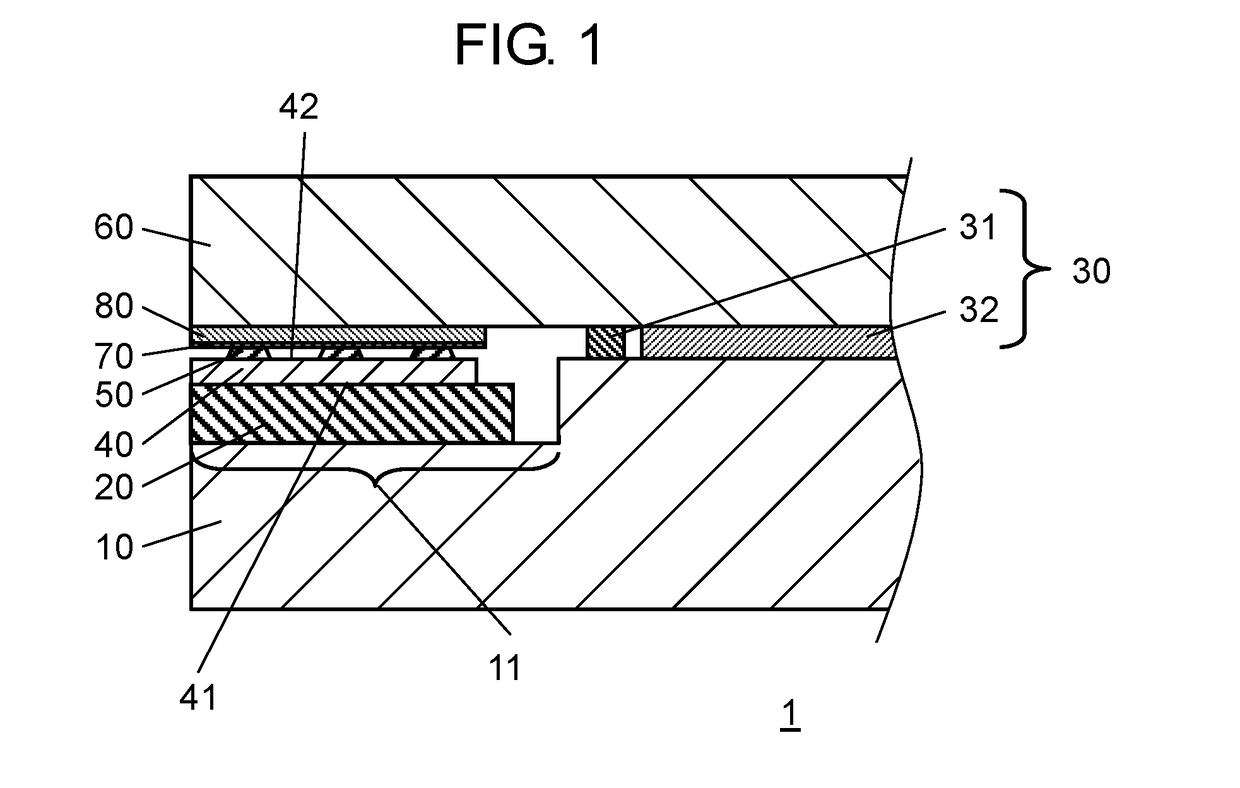
[0027]Hereinafter, a first exemplary embodiment of the present disclosure will be described with reference to FIG. 1 to FIG. 7.
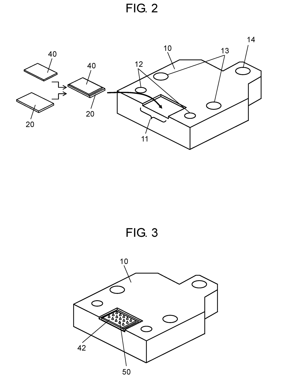
[0028]FIG. 1 is a cross-sectional view illustrating a schematic configuration of semiconductor laser device 1 according to the present embodiment. FIG. 2 to FIG. 7 are perspective views illustrating a method for manufacturing semiconductor laser device 1 according to the present embodiment.
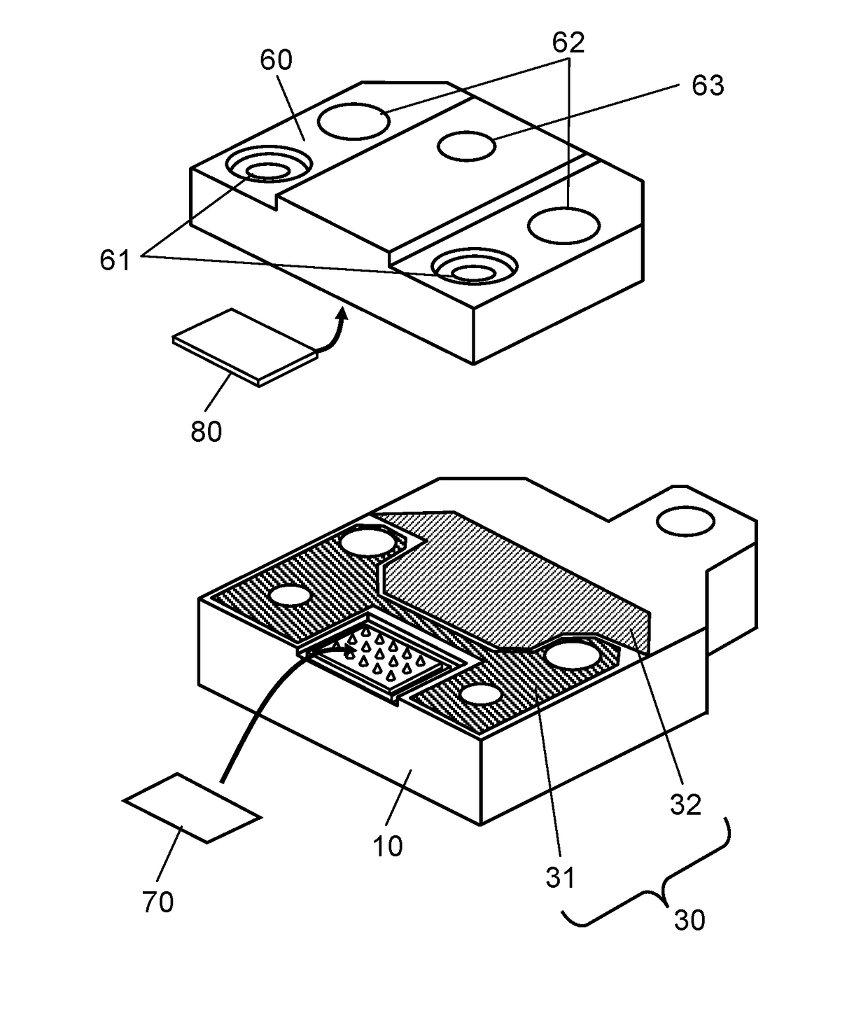
[0029]As illustrated in FIG. 1, semiconductor laser device 1 (semiconductor device) includes electrode block 10 (first electrode block), submount 20, insulating layer 30, semiconductor laser element 40 (semiconductor element), bump 50, and electrode block 60 (second electrode block). Furthermore, metal sheet 70 and metal layer 80 are provided in this order from bump 50 side between bump 50 and electrode block 60.
[0030]Electrode block 10 is electrically conductive, contains copper (Cu) as a main material, and is formed by plating a copper block with nickel (Ni) and gold (Au...
second exemplary embodiment
[0046]Next, a second exemplary embodiment of the present disclosure will be described with reference to FIG. 8 to FIG. 14. It should be noted that the same constituents as those of the first exemplary embodiment are given the same reference numerals, and the description of those constituents will be omitted. FIG. 8 is a cross-sectional view illustrating a schematic configuration of power semiconductor device 2 according to the present embodiment. FIG. 9 to FIG. 14 are perspective views illustrating a method for manufacturing power semiconductor device 2 according to the present embodiment.
[0047]In the first exemplary embodiment, semiconductor laser element 40 that outputs a laser beam is used as a semiconductor element, and semiconductor laser element 40 and submount 20 are mounted on an end portion of the upper surface of electrode block 10. By contrast, in the present embodiment, power semiconductor element 140 is used as a semiconductor element, and power semiconductor element 14...
third exemplary embodiment
[0061]Next, a third exemplary embodiment of the present disclosure will be described with reference to FIG. 15 and FIG. 16. It should be noted that the same constituents as those of the first exemplary embodiment are given the same reference numerals, and the description of those constituents will be omitted. FIG. 15 is a cross-sectional view illustrating a schematic configuration of semiconductor laser device 3 according to the present embodiment. FIG. 16 is a perspective view illustrating the schematic configuration of semiconductor laser device 3 according to the present embodiment.
[0062]In the first exemplary embodiment, recess 11 is provided in the upper surface of electrode block 10 on which submount 20 is mounted, and the lower surface of electrode block 60 facing the upper surface of electrode block 10 is flat. By contrast, in the present embodiment, the upper surface of electrode block 210 on which submount 20 is mounted is flat, and recess 261 is provided in the lower surf...
PUM
Abstract
A semiconductor device according to the present disclosure includes an electrically conductive first electrode block, an electrically conductive submount, an insulating layer, a semiconductor element, an electrically conductive bump, and an electrically conductive second electrode block. The submount is provided in a first region of the upper surface of the first electrode block, and electrically connected to the first electrode block. The semiconductor element is provided on the submount, and has a first electrode electrically connected to the submount. The bump is provided on the upper surface of a second electrode, opposite the first electrode, of the semiconductor element, and electrically connected to the second electrode. A third region of the lower surface of the second electrode block is electrically connected to the bump via an electrically conductive metal layer. An electrically conductive metal sheet is provided between the metal layer and the bump.
Description
TECHNICAL FIELD[0001]The present disclosure relates to a semiconductor device, and in particular to a semiconductor device mounted with a semiconductor element that generates much heat.BACKGROUND ART[0002]In recent semiconductor devices including a power semiconductor element or a semiconductor laser element, a larger electric current flows through the semiconductor element, and the amount of heat generated from the semiconductor element is increased accordingly. For example, in a high-power semiconductor laser device used for laserprocessing, a larger electric current flows through a semiconductor laser element mounted on the device in order to obtain a high-power laser beam, and the amount of heat generated from the semiconductor laser element is increased accordingly. When reaching a high temperature, semiconductor laser elements suffer performance degradation, such as a decrease in laser output. To stabilize the performance of semiconductor laser elements and prevent the overhe...
Claims
Application Information
Patent Timeline
Application Date:The date an application was filed.
Publication Date:The date a patent or application was officially published.
First Publication Date:The earliest publication date of a patent with the same application number.
Issue Date:Publication date of the patent grant document.
PCT Entry Date:The Entry date of PCT National Phase.
Estimated Expiry Date:The statutory expiry date of a patent right according to the Patent Law, and it is the longest term of protection that the patent right can achieve without the termination of the patent right due to other reasons(Term extension factor has been taken into account ).
Invalid Date:Actual expiry date is based on effective date or publication date of legal transaction data of invalid patent.

