Plasma display panel

Inactive Publication Date: 2009-06-25
FUJITSU HITACHI PLASMA DISPLAY LTD
View PDF5 Cites 0 Cited by
  • Summary
  • Abstract
  • Description
  • Claims
  • Application Information

AI Technical Summary

Benefits of technology

[0019]In accordance with the present invention, since an upper face of an auxiliary partition is partially made higher than a height of the upper face of a first wall section or the upper face of a second wall section of each of the partitions that divide a non-discharge region, it is possible to stably ensure a gas exhaust passage with a simple structure, and consequently provide a high-quality plasma display panel with high reliability.
[0020]In the present invention, paired substrates (for example, a frontside substrate and a backside substrate) include substrates made of glass, quartz and ceramics, and substrates with desired constituent elements, such as an electrode, an insulating film, a dielectric layer and a protective film, formed on these substrates.
[0021]A plurality of display electrodes may include any display electrodes formed on one of substrates (for example, the frontside substrate) so as to extend in a predetermined direction. Moreover, a plurality of address electrodes may include any address electrodes formed on the other substrate (for example, the backside substrate) so as to extend in a direction intersecting with the display electrodes on one of the substrates.
[0022]The display electrodes and the address electrodes may be formed by using any kinds of materials and methods conventionally known in a corresponding field. Examples of materials used for these electrodes include transparent conductive materials, such as ITO and SnO2, and metal conductive materials, such as Ag, Au, Al, Cu, and Cr. Various kinds of methods known in the corresponding field may be applied to a method for forming the electrodes. For example, a thick-film-forming technique such as a screen-printing process may be used, and a thin-film-forming technique including a physical deposition method, such as a vapor deposition method and a sputtering method, or a chemical deposition method such as a thermal CVD method and a photo CVD method, may be used.

Problems solved by technology

In this structure, since a slit width and a reverse slit width are the same, it becomes difficult to carry out a driving operation by using the same driving method as a method for a structure with a wide reverse slit side.
In this method, however, since a complicated driving sequence for addressing so as to set display contents is required, and since no reverse slit is present, with the display electrodes being associated with two adjacent lines in a longitudinal direction, a discharge interference tends to occur between adjacent display cells.

Method used


Image

  • Plasma display panel
  • Plasma display panel
  • Plasma display panel

Examples


first embodiment

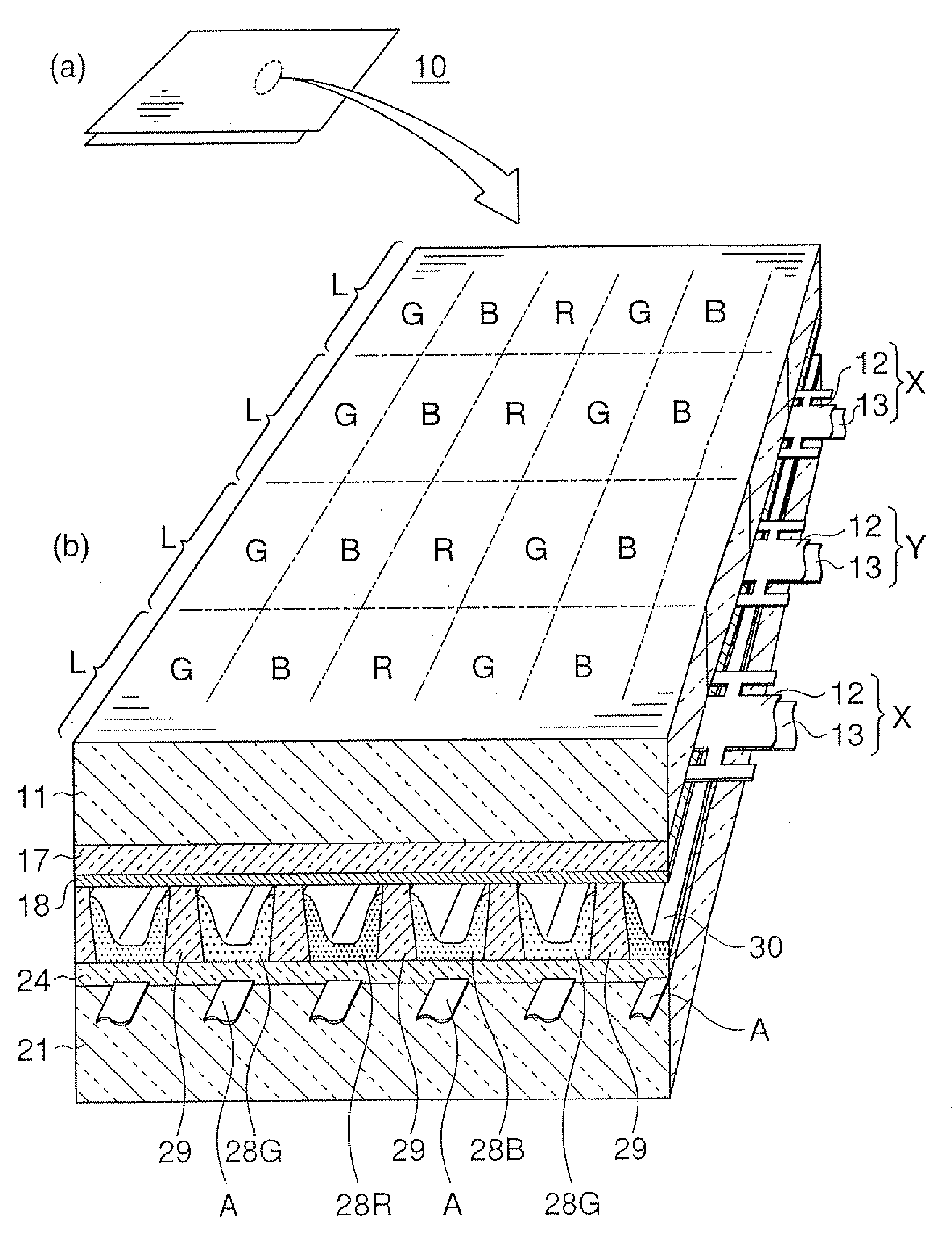
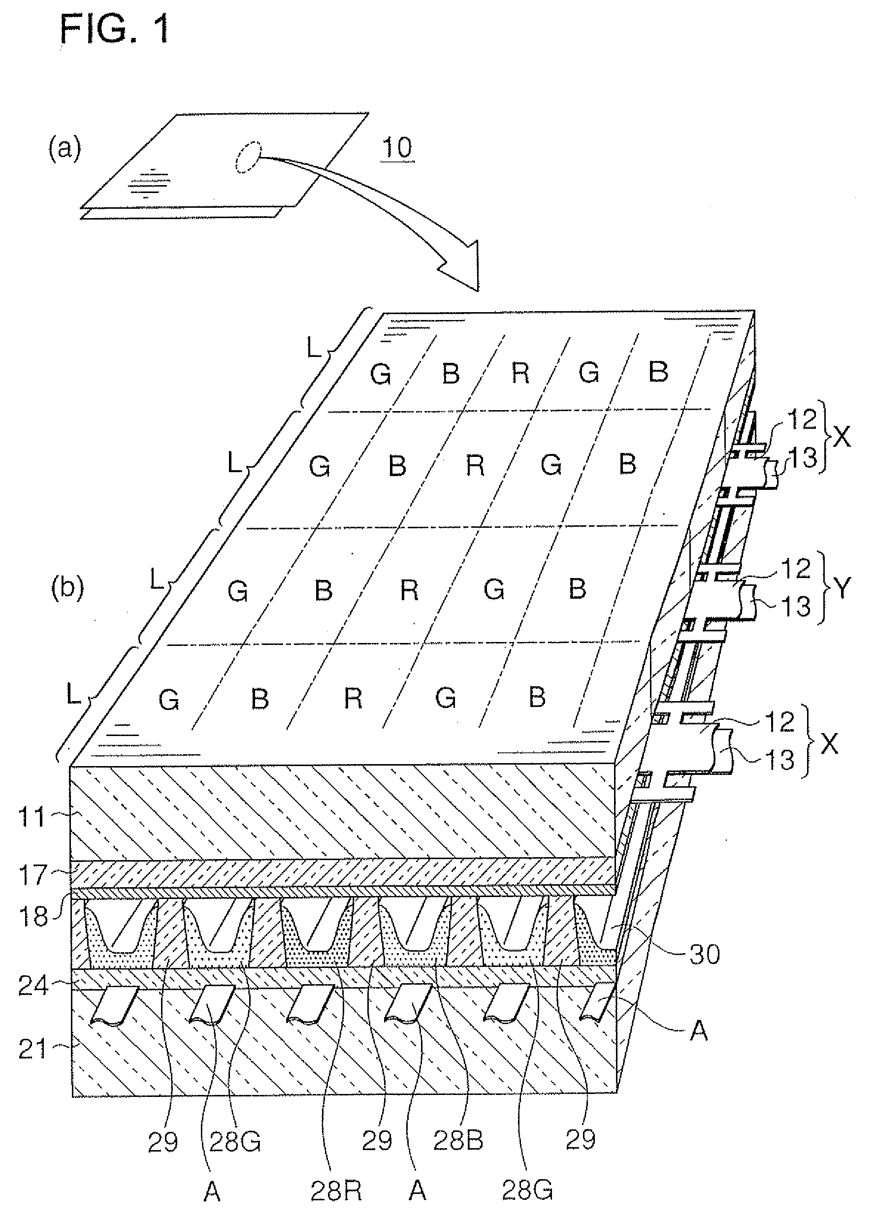
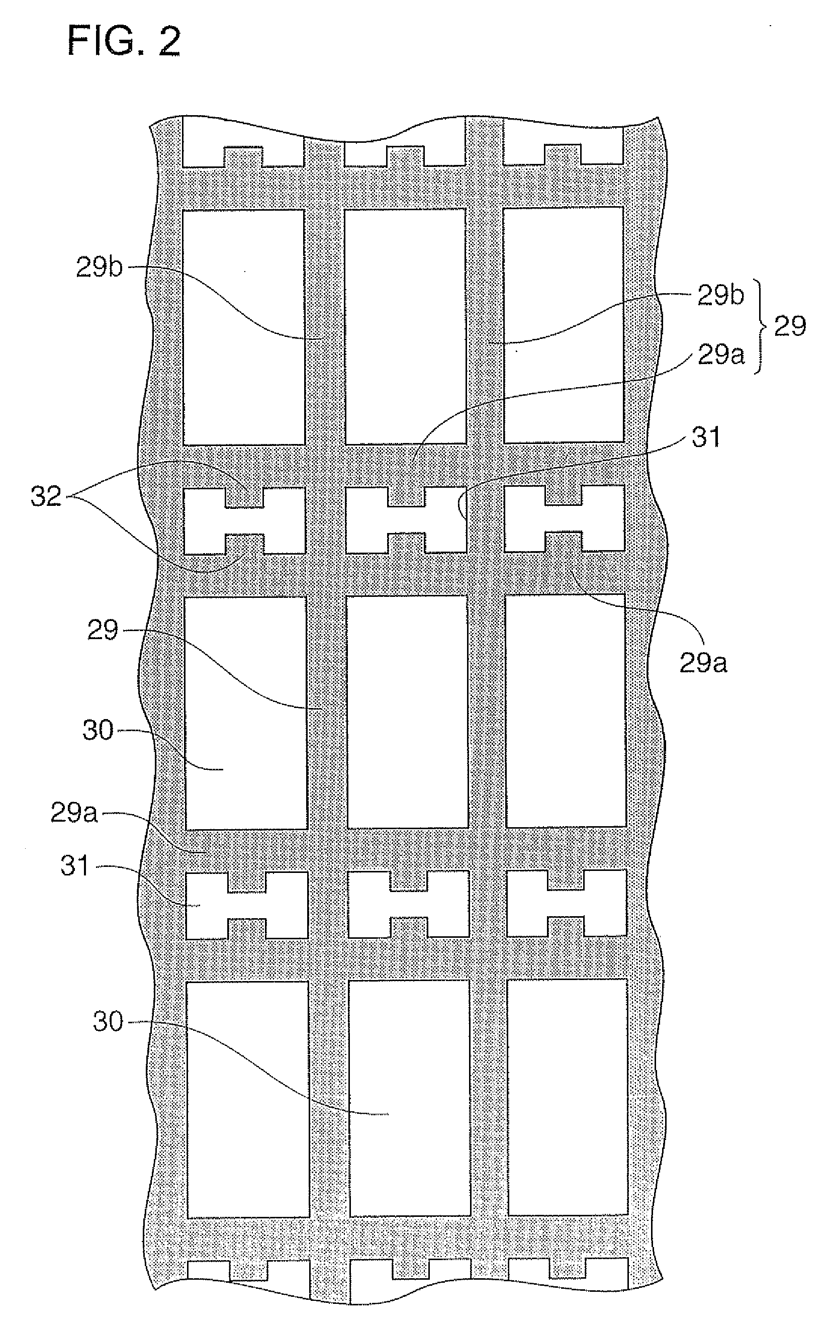
[0074]FIGS. 2 and 3 show a positional relationship between a partition structure and display electrodes of a first embodiment of a PDP in accordance with the present invention. In this PDP, first display electrodes X and second display electrodes Y serving as sustain discharge electrodes are disposed in an order of X·Y·X·Y . . . . Here, a gap between the display electrode X and the display electrode Y is formed into a display cell. This PDP is provided with a plurality of partitions 29 formed as a mesh shape by using a sand blasting method. Each partition 29 is configured by lateral wall sections 29a serving as first wall sections that extend in a line direction (a direction in which the display electrodes X, Y are formed) and longitudinal wall sections 29b serving as second wall sections that extend in a column direction (a direction that intersects with the direction in which the display electrodes X, Y are formed).

[0075]The partitions 29 are formed through processes in which, aft...

second embodiment

[0086]FIG. 5 is a plan view that shows partitions and auxiliary partitions of a second embodiment of a PDP in accordance with the present invention. That is, in the second embodiment, paired auxiliary partitions 33, 33 opposing to each other are allowed to protrude toward the inside of each non-discharge region 31 from the longitudinal wall sections 29b of partitions 29 that face the non-discharge region 31.

[0087]Here, in the first embodiment and the second embodiment, two auxiliary partitions 32, 32 (33, 33) are formed for each single non-discharge region 31. However, the number of the auxiliary partitions to be formed in each non-discharge region 31 may be set to one, or may be set to three or more.

third embodiment

[0088]FIG. 6 is a plan view that shows partitions and auxiliary partitions of a third embodiment of a PDP in accordance with the present invention. The third embodiment differs from the first embodiment in that a plurality of non-discharge regions 31, 31, 31 corresponding to gap portions between adjacent lines in the line direction are allowed to communicate with one another, and in that the auxiliary partitions 34, 34 opposing to each other are allowed to protrude from the lateral wall sections 29a toward the inside of each of the non-discharge regions 31, 31 that communicate with one another, at each intersection point between the longitudinal wall sections 29b and the lateral wall sections 29a.

[0089]With this arrangement, not only the gas exhaust passage formed by the height difference generated between the lateral wall section 29a and the auxiliary partition 34 of each of the partitions 29, but also a gas exhaust passage that extends in a lateral direction (in a direction cross...


PUM


Abstract

A high-definition, high-reliability plasma display panel having a simple structure and having a stably ensured gas-exhaust passage. In the plasma display panel, display electrodes and address electrodes crossing these display electrodes are provided between a pair of substrate defining an electric discharge space, display lines produced by surface discharge are provided between adjacent display electrodes, discharge luminous regions are provided at cross sections between display lines and address electrodes, partitions (29) for defining discharge luminous regions for each line and for each column by first wall sections (29a) extending in the line direction in which the display electrodes are provided and second wall sections (29b) extending in the column direction in which the address electrodes are provided, nondischarge regions (31) are formed at interlinear sections which are sections between adjacent display lines, auxiliary partitions (32) projecting the first or second wall sections (29a or 29b) of the partitions (29) defining the nondischarge region (31) are formed by baking a material having a thermal shrinkability. Since the thermal shrinkage by the baking in the height direction is uneven, the height of the top part is partially greater than those of the top parts of the first and second partitions (29a, 29b) of the partitions defining the nondischarge regions (31).

Description

TECHNICAL FIELD[0001]This invention relates to a plasma display panel (PDP), and more particularly relates to a PDP that has partitions for defining discharge light-emission regions for each line and for each column.BACKGROUND ART[0002]At present, PDPs of an AC-drive type that are generally commercialized are those of a surface-discharge type. Herein, “surface-discharge type” refers to a type of structure in which first and second display electrodes, which respectively form cathodes and anodes so as to perform a display discharge as a main discharge, are arranged on a substrate on a front face side or a back face side respectively in parallel with each other.[0003]In a surface-discharge-type PDP, phosphor layers used for color display can be disposed apart from paired display electrodes in a panel thickness direction, and with this arrangement, it is possible to reduce degradation of the phosphor layers due to ion impact at the time of discharging. Therefore, in comparison with a co...

Claims


Application Information

Patent Timeline
IPC IPC(8): H01J17/49H01J11/12H01J11/36
CPCH01J11/12H01J11/36H01J2211/54H01J2211/365H01J2211/361
Inventor OHIRA, KOJISAWA, MASAHIRO
Owner FUJITSU HITACHI PLASMA DISPLAY LTD
Why Eureka
Try Eureka