Integrated circuit with ion sensitive sensor and manufacturing method

Active Publication Date: 2013-12-19
NXP BV
View PDF2 Cites 9 Cited by
  • Summary
  • Abstract
  • Description
  • Claims
  • Application Information

AI Technical Summary

Benefits of technology

The present invention provides a method for manufacturing an IC at a reduced cost. The method includes using a metallization stack with a first patterned metal layer and a second patterned metal layer. The second patterned metal layer includes a plurality of further apertures. The method further includes forming the plurality of apertures by extending each sample volume through one of the further apertures such that the sample volume terminates at one of the electrodes. This results in a high-resolution lithography step that is easier to achieve and without having to planarize the passivation layer, if present.

Problems solved by technology

Apart from the technical challenges of the miniaturization, i.e. how to reliably reproduce detection techniques in the IC domain, a major hurdle that needs overcoming en-route to the successful commercialization of such lab-on-chip solutions is the manufacturing cost of such ICs.
These factors are often correlated; a high manufacturing complexity, e.g. a large number of process steps, negatively affects the process yield, such that relatively complex ICs are typically costly to manufacture, as a large number of process steps is required and the yield of the process is relatively low.
In addition, the manufacturing complexity significantly complicates further miniaturization of the IC, e.g. for the purpose of increasing the sensor density on the IC or for the purpose of porting the IC design to a smaller technology.
However, a particular drawback of the IC disclosed in US 2010 / 0137143 A1 is that it requires a relatively large number of additional process steps to manufacture, which adds to the cost of the IC.
Also, the fact that the passivation layer is used as the pH sensitive material on the extended gate electrodes of the field effect transistors (FETs) in the metallization stack is not ideal as it limits the materials that can be used for the passivation layer to pH-sensitive materials and moreover limits the sensitivity of the FETs due to the fact that the passivation layer is required to have a minimum thickness in order to effectively protect the underlying structures of the IC from external influences.

Method used


Image

  • Integrated circuit with ion sensitive sensor and manufacturing method
  • Integrated circuit with ion sensitive sensor and manufacturing method
  • Integrated circuit with ion sensitive sensor and manufacturing method

Examples


Embodiment Construction

[0025]Embodiments of the invention are described in more detail and by way of non-limiting examples with reference to the accompanying drawings, wherein:

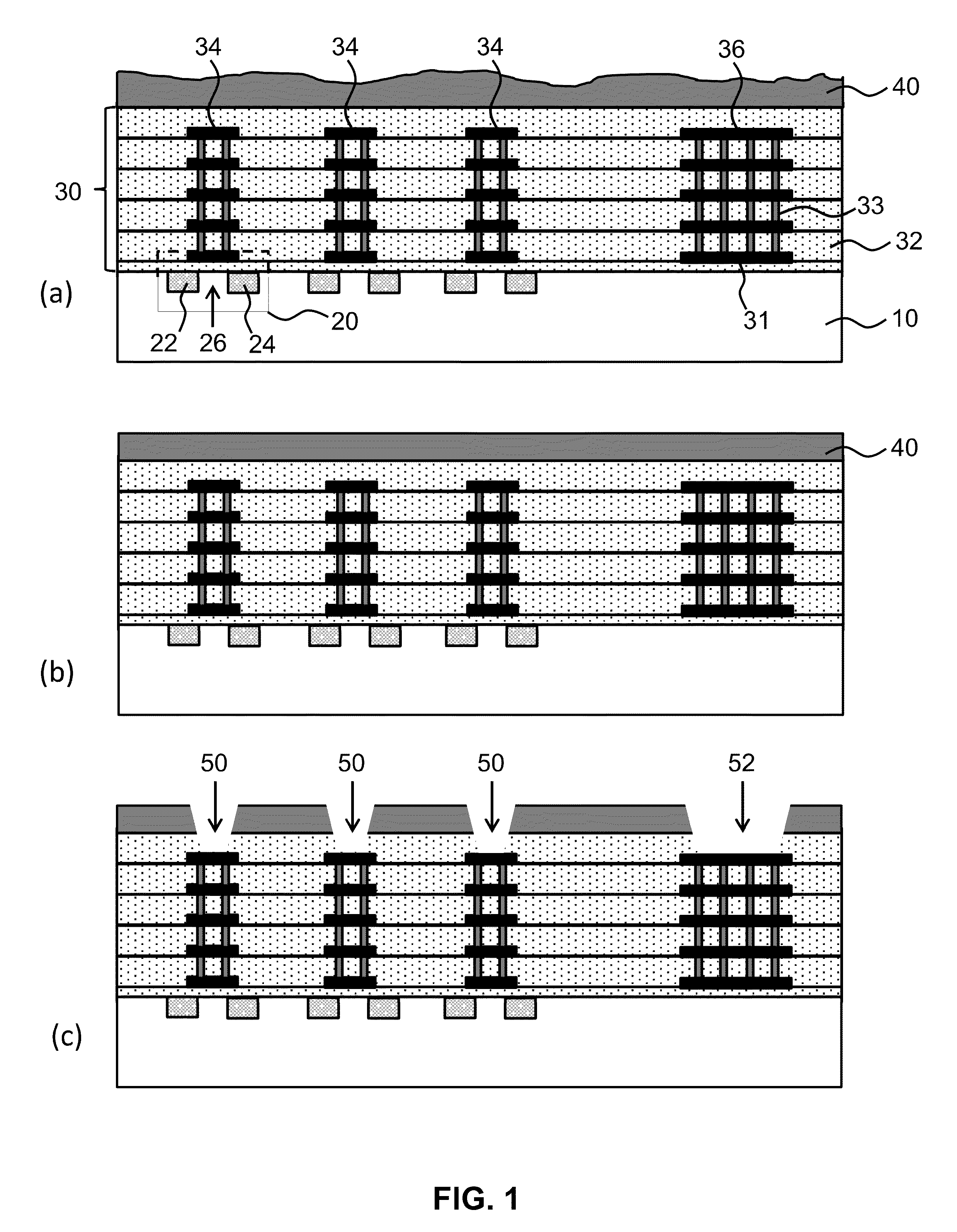
[0026]FIG. 1 schematically depicts an embodiment of a method of the present invention;

[0027]FIG. 2 schematically depicts an alternative embodiment of a method of the present invention; and

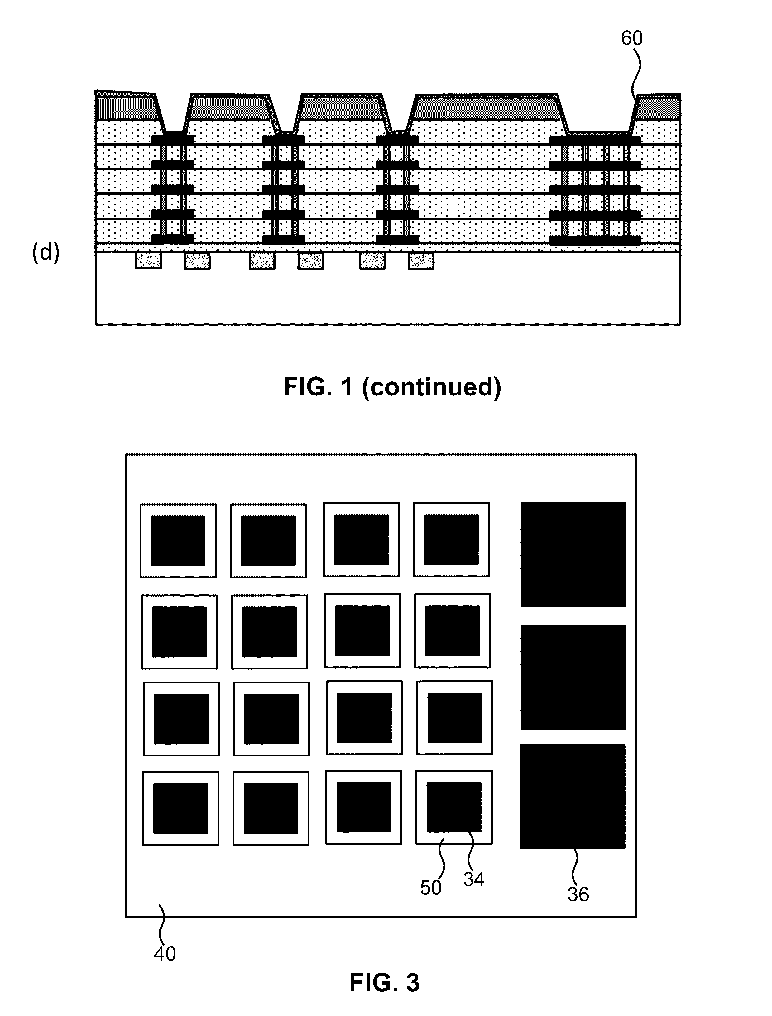
[0028]FIG. 3 shows a top view of an IC according to an embodiment of the present invention.

DETAILED DESCRIPTION OF THE DRAWINGS

[0029]It should be understood that the Figures are merely schematic and are not drawn to scale. It should also be understood that the same reference numerals are used throughout the Figures to indicate the same or similar parts.

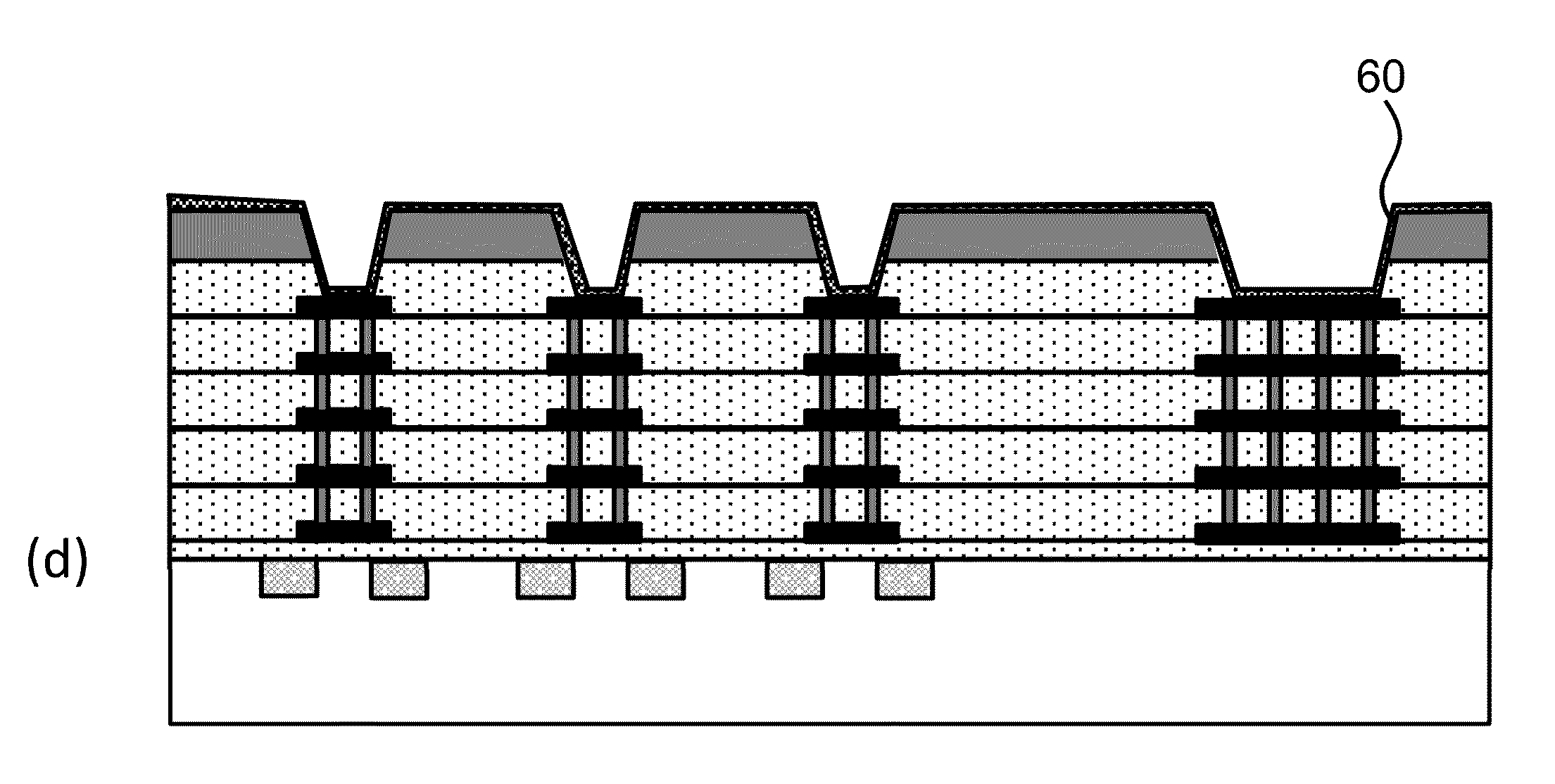
[0030]FIG. 1 schematically depicts an embodiment of a method according to the present invention for manufacturing an IC comprising a plurality of ion-sensitive electrodes such as pH-sensitive electrodes in the back end of line (BEOL), more specifically in the metallization stack of the IC. Preferably...


PUM


Abstract

Disclosed is an integrated circuit comprising a substrate (10) carrying plurality of circuit elements (20); a metallization stack (30) over said substrate for providing interconnections to at least some of said circuit elements, the metallization stack comprising a plurality of patterned metal layers (31) spatially separated from each other by respective electrically insulating layers (32), at least some of said electrically insulating layers comprising conductive portions (33) that electrically interconnect portions of adjacent metal layers, wherein at least one of the patterned metallization layers comprises a plurality of ion-sensitive electrodes (34), each ion-sensitive electrode being electrically connected to at least one of said circuit elements, a plurality of sample volumes (50) extending into said metallization stack, each sample volume terminating at one of said ion-sensitive electrodes; and an ion-sensitive layer lining at least the ion-sensitive electrodes in said sample volumes. A method of manufacturing such an IC is also disclosed.

Description

FIELD OF THE INVENTION[0001]The present invention relates to an integrated circuit (IC) comprising a plurality of ion-sensitive electrodes in the metallization stack of the IC.[0002]The present invention further relates to a method of manufacturing such an IC.BACKGROUND OF THE INVENTION[0003]The on-going diversification of IC functionality has led to the miniaturization of many techniques, i.e. has made many techniques available on an IC. Examples of such miniaturization include (medical) laboratory techniques such as analyte analysis of bodily fluid samples and DNA sequencing techniques.[0004]Apart from the technical challenges of the miniaturization, i.e. how to reliably reproduce detection techniques in the IC domain, a major hurdle that needs overcoming en-route to the successful commercialization of such lab-on-chip solutions is the manufacturing cost of such ICs. The manufacturing cost is in part dominated by the following two factors: process complexity and process yield. The...

Claims


Application Information

Patent Timeline
IPC IPC(8): H01L29/66
CPCH01L29/66H01L29/66007G01N27/4145G01N27/4148
Inventor MERZ, MATTHIASJUFFERMANS, CASPERNACKAERTS, AXEL
Owner NXP BV
Why Eureka
Try Eureka