Integrated circuit with sensors and manufacturing method

a technology of integrated circuits and sensors, applied in the field of integrated circuits, can solve the problems of limiting the sensitivity of fets, increasing the cost of ic, and a large number of additional process steps, and achieve the effect of high-resolution lithography

Active Publication Date: 2013-12-26
NXP BV
View PDF2 Cites 75 Cited by
  • Summary
  • Abstract
  • Description
  • Claims
  • Application Information

AI Technical Summary

Benefits of technology

[0027]However, in a preferred alternative embodiment, the metallization stack further comprises a first patterned metal layer and a second patterned metal layer over the first patterned metal layer, said first patterned metal layer comprising the plurality of electrodes and the second patterned metal layer comprising a plurality of further apertures, wherein the step of forming the plurality of apertures further comprises extending each well through one of the further apertures such that said sample volume terminates at one of the sensing electrodes, as in this case a high-resolution lithography step can be achieved more easily as well as without having to first planarize the passivation layer.

Problems solved by technology

Firstly, it requires a relatively large number of additional process steps to manufacture, which adds to the cost of the IC.
The fact that the passivation layer is used as the pH sensitive material on the extended gate electrodes of the field effect transistors (FETs) in the metallization stack is a further concern as it limits the materials that can be used for the passivation layer to pH-sensitive materials and moreover limits the sensitivity of the FETs due to the fact that the passivation layer is required to have a minimum thickness in order to effectively protect the underlying structures of the IC from external influences.

Method used


Image

  • Integrated circuit with sensors and manufacturing method
  • Integrated circuit with sensors and manufacturing method
  • Integrated circuit with sensors and manufacturing method

Examples


Embodiment Construction

[0028]Embodiments of the invention are described in more detail and by way of non-limiting examples with reference to the accompanying drawings, wherein:

[0029]FIG. 1 schematically depicts an embodiment of a method of the present invention;

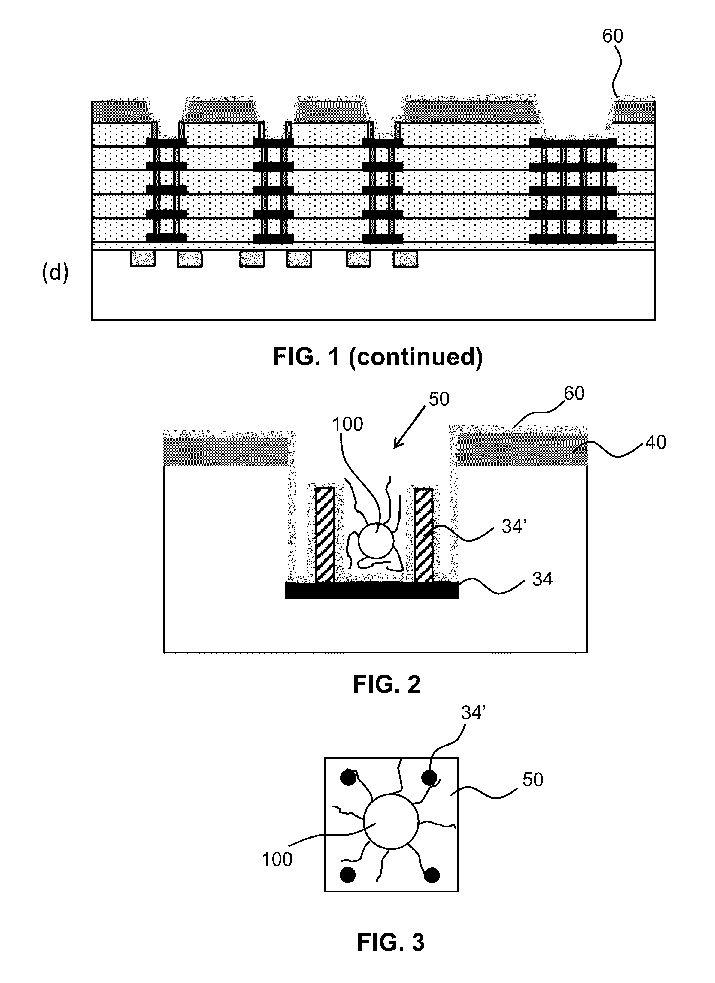
[0030]FIGS. 2 and 3 schematically depict a cross section and a top view respectively of a sensing well of an IC of the present invention loaded with a bead;

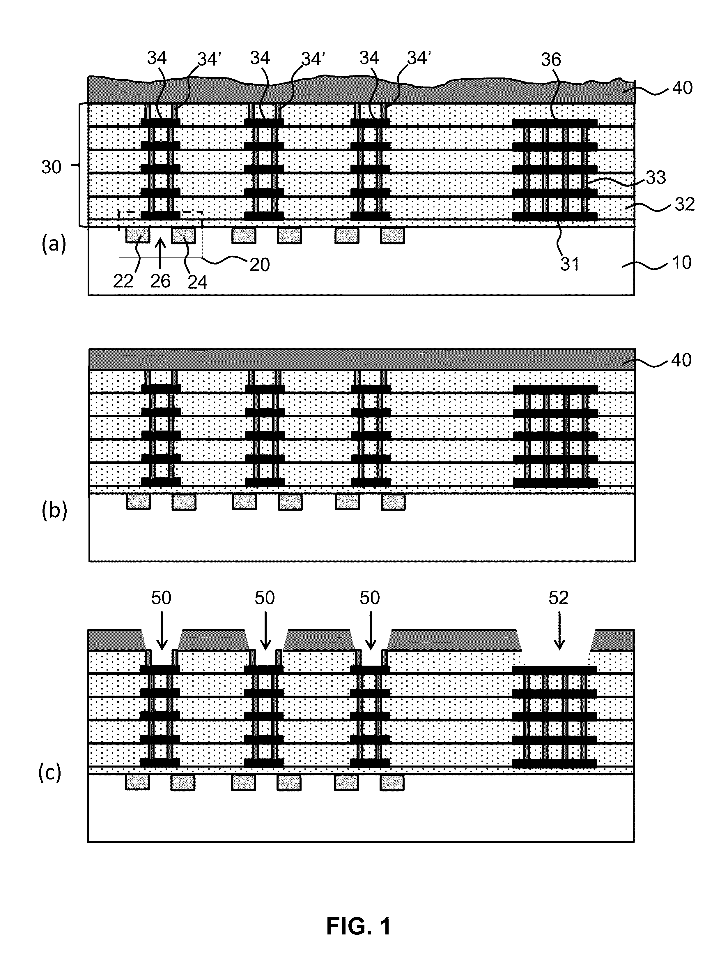
[0031]FIG. 4 schematically depicts an alternative embodiment of a method of the present invention; and

[0032]FIG. 5 shows a top view of an IC according to an embodiment of the present invention.

DETAILED DESCRIPTION OF THE DRAWINGS

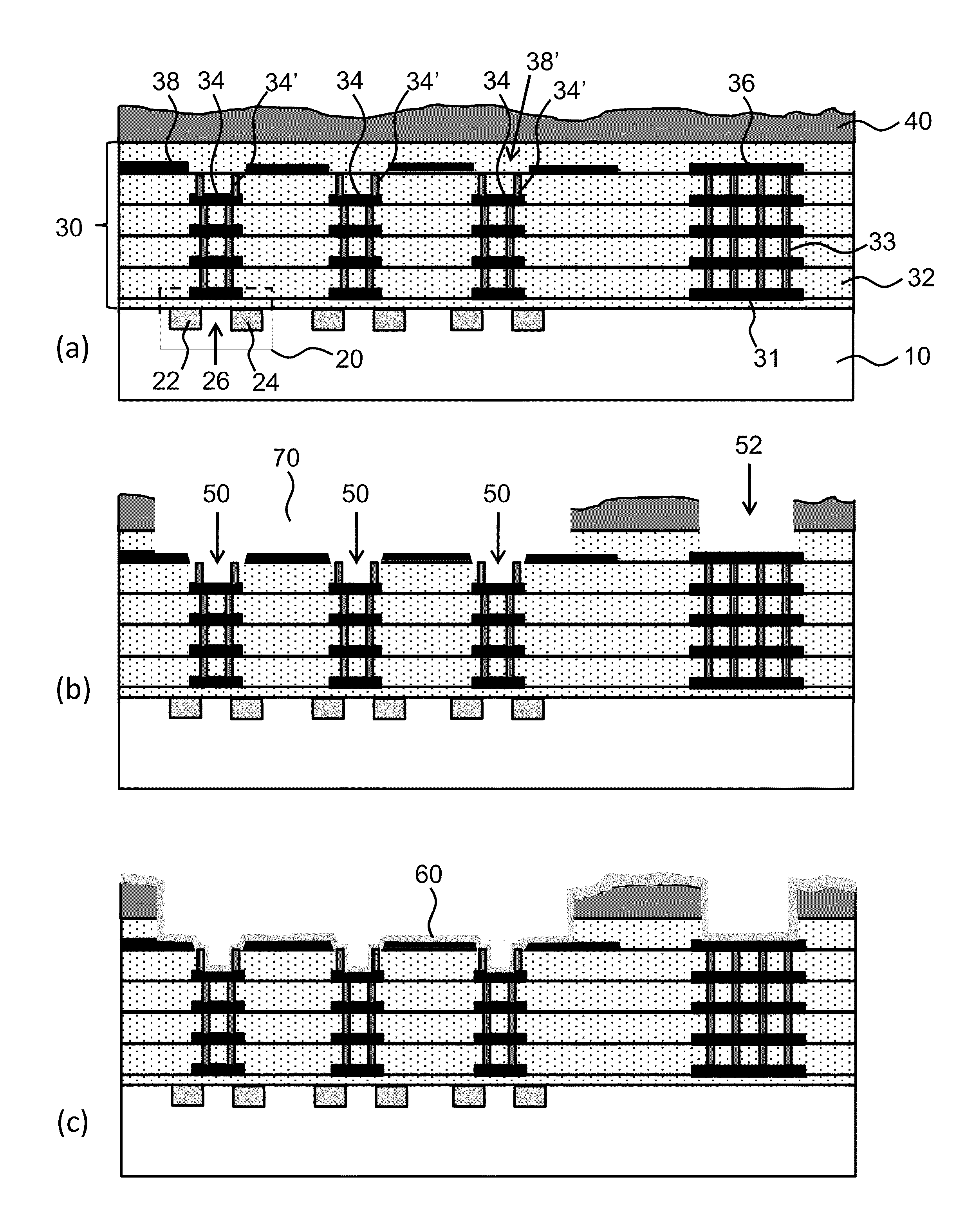
[0033]It should be understood that the Figures are merely schematic and are not drawn to scale. It should also be understood that the same reference numerals are used throughout the Figures to indicate the same or similar parts.

[0034]FIG. 1 schematically depicts an embodiment of a method according to the present invention for manufacturing an IC comprising a plurality of...


PUM

PropertyMeasurementUnit
thicknessaaaaaaaaaa
thicknessaaaaaaaaaa
thicknessaaaaaaaaaa

Abstract

Disclosed is an integrated circuit comprising a substrate (10) carrying plurality of circuit elements (20); a plurality of sensing electrodes (34) over said substrate, each sensing electrode being electrically connected to at least one of said circuit elements; and a plurality of wells (50) for receiving a sample, each sensing electrode defining the bottom of one of said wells, wherein each sensing electrode comprises at least one portion (34′) extending upwardly into said well. A method of manufacturing such an IC is also disclosed.

Description

FIELD OF THE INVENTION[0001]The present invention relates to an integrated circuit (IC) comprising a plurality of ion-sensitive electrodes in the metallization stack of the IC.[0002]The present invention further relates to a method of manufacturing such an IC.BACKGROUND OF THE INVENTION[0003]The on-going diversification of IC functionality has led to the miniaturization of many techniques, i.e. has made many techniques available on an IC. Examples of such miniaturization include (medical) laboratory techniques such as analyte analysis of bodily fluid samples and DNA sequencing techniques.[0004]An example of a lab-on-chip device for the monitoring of DNA sequencing is disclosed in US 2010 / 0137143 A1. This document discloses a CMOS IC in which a plurality of pH-sensitive electrodes, i.e. pH-sensitive gate electrodes of a plurality of ChemFETs or ISFETs is located in the upper metal layer of the metallization stack of the IC. A passivation layer is formed over the metallization stack, ...

Claims


Application Information

Patent Timeline
Patent Type & Authority Applications(United States)
IPC IPC(8): G01N27/26H01L21/82
CPCG01N27/26H01L21/82G01N27/4145G01N27/4148B01L2300/0893B01L2200/12B01L2300/0645B01L2300/0819B01L3/5085
Inventor MERZ, MATTHIAS
Owner NXP BV
Why Eureka
Try Eureka