

Memory device and redundancy method thereof
a memory device and redundancy technology, applied in semiconductor devices, digital storage, instruments, etc., can solve the problems of increasing difficulty in manufacturing memory elements without failures or defects, and achieve the effect of reducing the area of the peripheral circuit, high speed, and simplifying the structure of the peripheral circui
- Summary
- Abstract
- Description
- Claims
- Application Information
AI Technical Summary
Benefits of technology
Problems solved by technology
Method used
Image

Examples
Embodiment Construction
[0035]The following description is of the best-contemplated mode of carrying out the invention. This description is made for the purpose of illustrating the general principles of the invention and should not be taken in a limiting sense. The scope of the invention is best determined by reference to the appended claims.
[0036]The embodiments of the invention are described below with references made to the accompanying drawings. Here, an example of a NAND-type flash memory is used as a preferred embodiment. In addition, to be noted, for simplicity and clarity, the elements in the Figures may be enlarged and have different proportions from that in the practical situation.
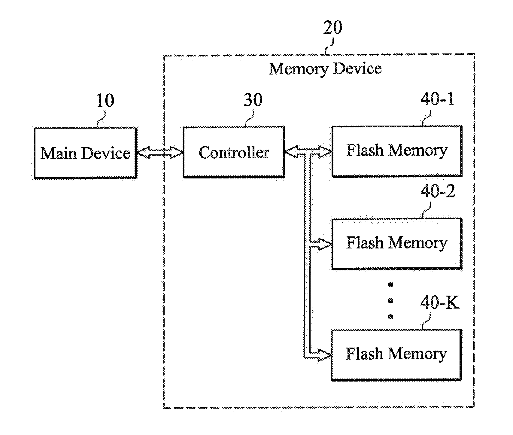
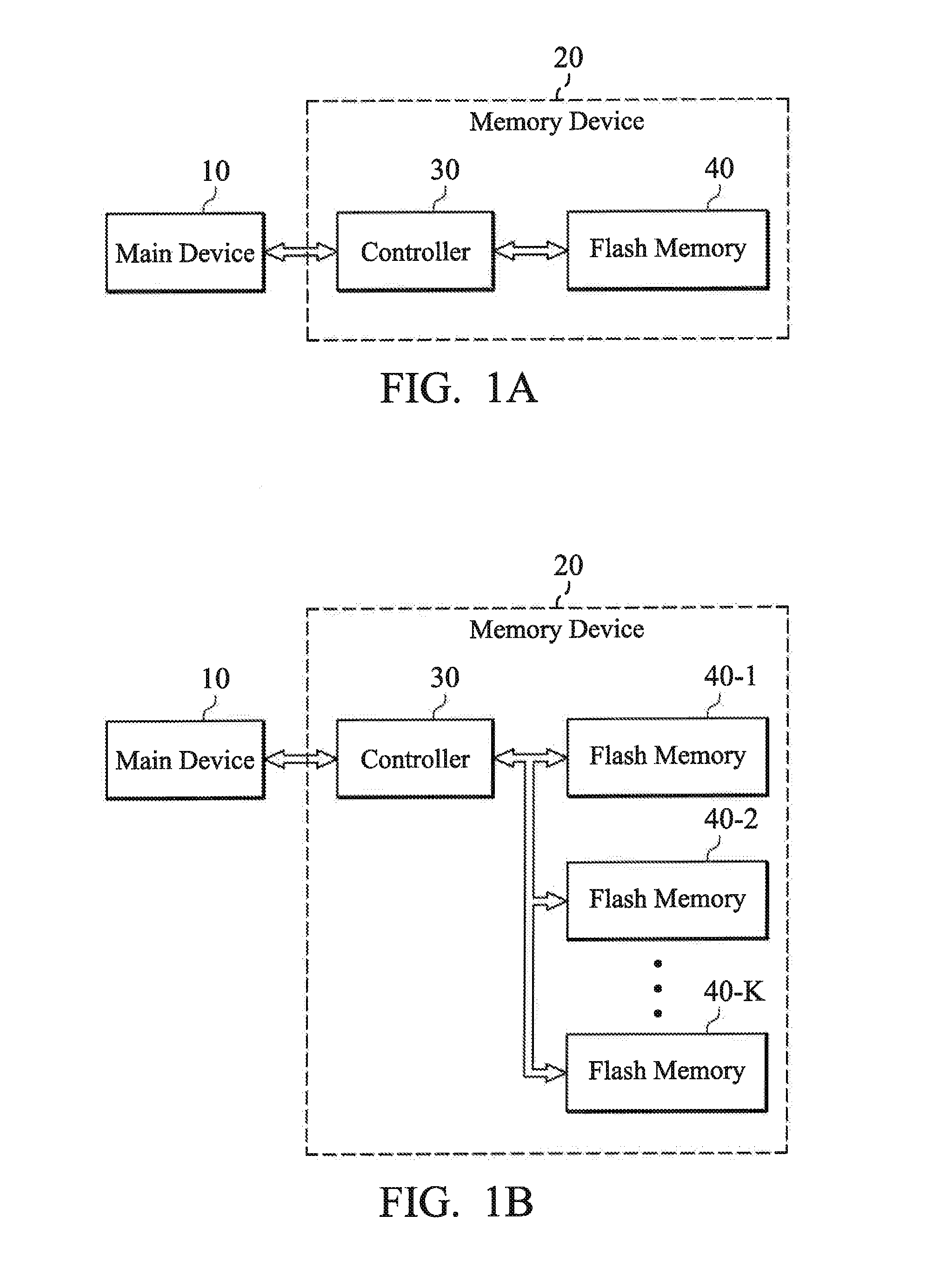
[0037]FIG. 1 is a block diagram of a memory device according to an embodiment of the invention. A memory device 20 is connected to a main device 10. The memory device 20 responds to requests of the main device 10. The memory device 20 comprises a controller 30 and a flash memory 40. The controller 30 responds to command...
PUM
 Abstract
Description
Claims
Application Information