Method of manufacturing dual damascene structure

a damascene and structure technology, applied in the direction of semiconductor/solid-state device manufacturing, basic electric elements, electric apparatus, etc., can solve the problems of reducing the yield of the later formed semiconductor devices, adversely affecting the later manufacturing process, and reducing the correctness of the formed first pattern, so as to achieve the effect of improving the consistency and precise patterns of the dual damascene structur

Active Publication Date: 2013-12-19
UNITED MICROELECTRONICS CORP
View PDF2 Cites 40 Cited by
  • Summary
  • Abstract
  • Description
  • Claims
  • Application Information

AI Technical Summary

Benefits of technology

[0008]An objective of the present invention is therefore to provide a method of fabricating a dual damascene structure adopting the double patterning technique (DPT) to improve the completeness of the dual damascene structure.
[0010]As DPT is implemented in the present invention to form the trench openings and the via openings by respectively performing at least four patterning processes, the dielectric layer is totally covered by the dielectric mask layer to prevent the dielectric layer from being affected by the four patterning processes, for example, the dielectric layer may not absorb the etchants used in the patterning processes, this way the material characteristics of the dielectric layer can be maintained. Additionally, in the present invention, after the trench openings and the via openings are sequentially formed in the mask layers, the trench openings and the via openings in the mask layers are simultaneously transferred to the dielectric layer to avoid the effects caused by the etchants or the photoresist of the repeated patterning processes. Accordingly, precise patterns can be obtained, and the consistency of the dual damascene structure may be improved.

Problems solved by technology

However, after the first lithography process, the target layer having the first pattern formed thereon may directly contact the cleaning solution, the etchant or the chemical solvent used in the second lithography process, and the formed first pattern in the target layer may be deformed or the exposed surface of the target layer may be damaged, which may reduce the correctness of the formed first pattern and adversely affect the later manufacturing processes.
For example, in the damascene process of the metal interconnect, the openings of the first pattern may not be capable of being filled with the conductive material and voids may be formed between the conductive material and the target layer due to the deformation of the first pattern, and the yield of the later formed semiconductor devices decreases.
Consequently, how to improve the patterning process for obtaining complete patterns is still an important issue in the field.

Method used


Image

  • Method of manufacturing dual damascene structure
  • Method of manufacturing dual damascene structure
  • Method of manufacturing dual damascene structure

Examples


Embodiment Construction

[0013]To provide a better understanding of the present invention, preferred exemplary embodiments will be described in detail. The preferred exemplary embodiments of the present invention are illustrated in the accompanying drawings with numbered elements.

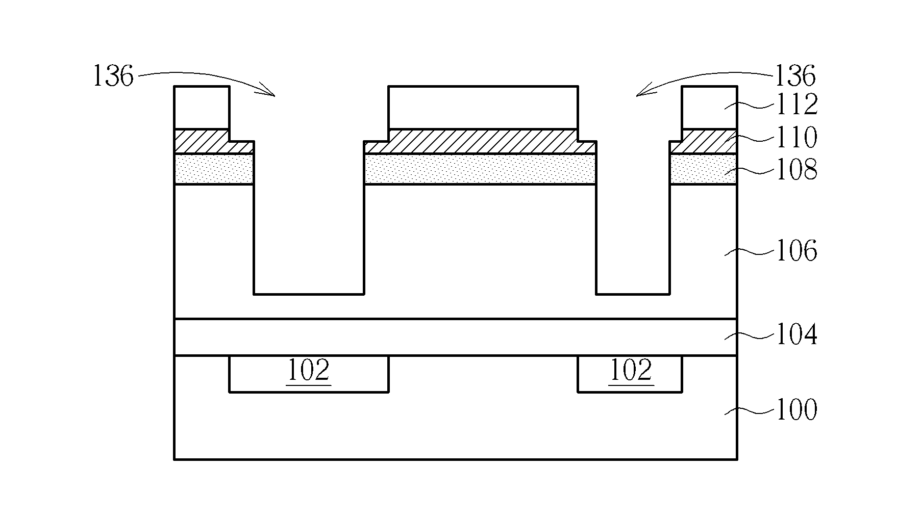
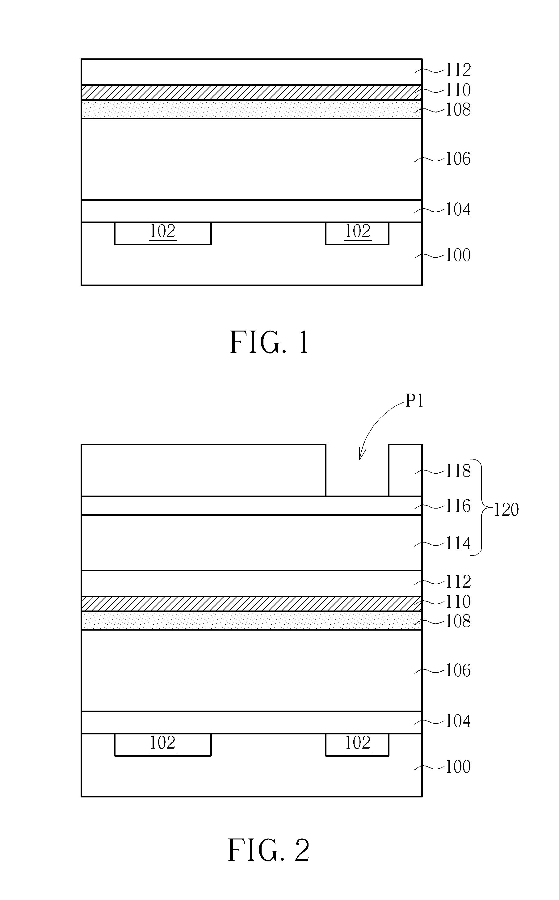
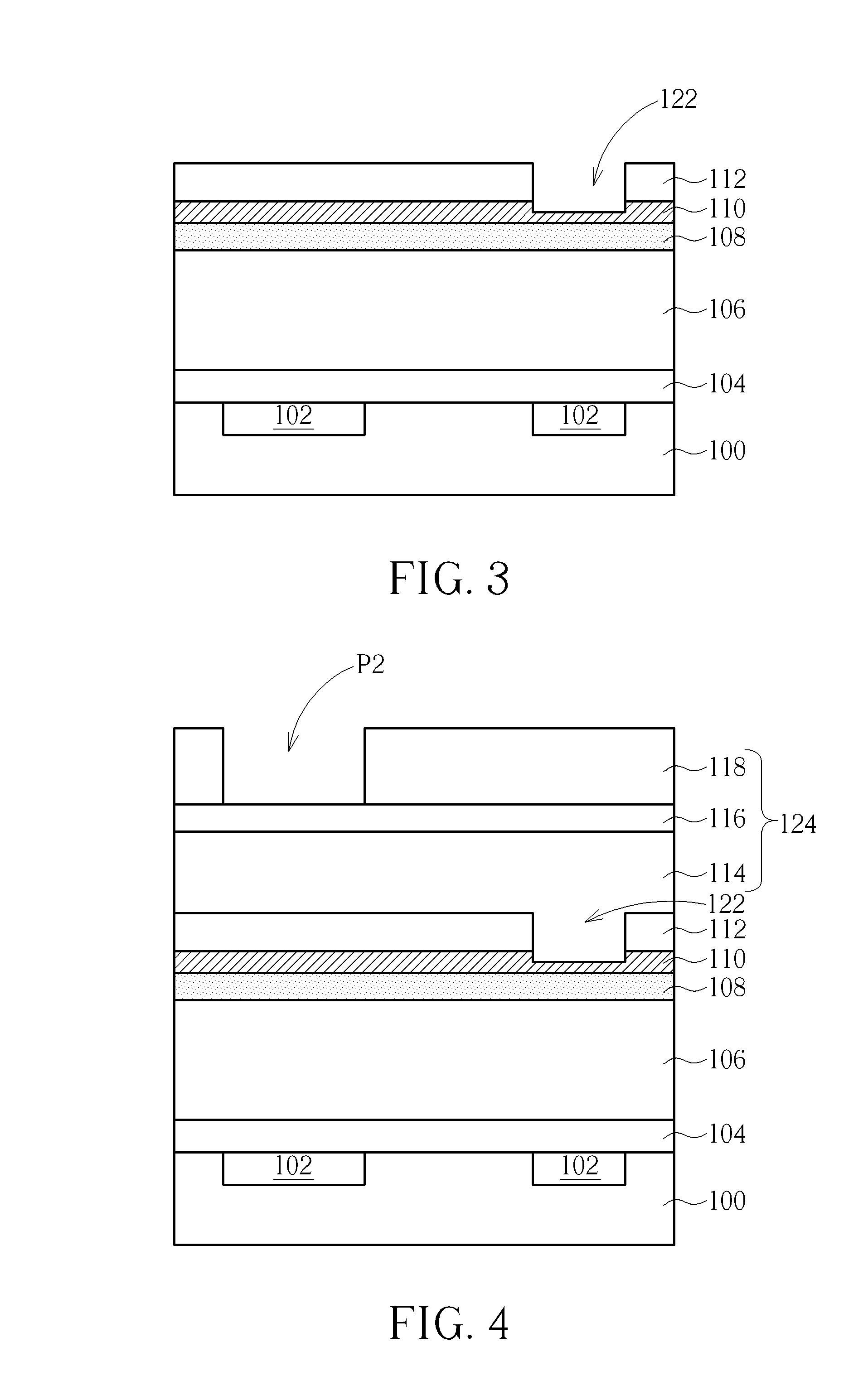
[0014]The present invention provides a method of fabricating a dual damascene structure. Please refer to FIG. 1 through FIG. 14, which are schematic diagrams illustrating a method of fabricating a dual damascene structure according to a preferred exemplary embodiment of the present invention. As shown in FIG. 1, a substrate 100 is provided, and the substrate 100 includes a plurality of conductive layers 102 and a base layer 104 covering the conductive layers 102. The substrate 100 may include other semiconductor elements (not shown). The conductive layers 102 could be any kind of conductive elements, including gate electrodes, source electrodes, contact plugs, via plugs, conductive lines etc., or metal contacts. Furthermore, the ba...


PUM

PropertyMeasurementUnit
thicknessaaaaaaaaaa
roughnessaaaaaaaaaa
widthaaaaaaaaaa

Abstract

A method for fabricating a dual damascene structure includes the following steps. At first, a dielectric layer, a dielectric mask layer and a metal mask layer are sequentially formed on a substrate. A plurality of trench openings is formed in the metal mask layer, and a part of the metal mask layer is exposed in the bottom of each of the trench openings. Subsequently, a plurality of via openings are formed in the dielectric mask layer, and a part of the dielectric mask layer is exposed in a bottom of each of the via openings. Furthermore, the trench openings and the via openings are transferred to the dielectric layer to form a plurality of dual damascene openings.

Description

BACKGROUND OF THE INVENTION[0001]1. Field of the Invention[0002]The present invention relates to a method of fabricating a dual damascene structure, and more particularly, to a method of fabricating a dual damascene structure adopting the double patterning technique (DPT).[0003]2. Description of the Prior Art[0004]In the fabrication of semiconductor integrated circuits (ICs), semiconductor devices are generally connected by several metallic interconnecting layers commonly referred to as multi-level interconnects, and a damascene process is a convenient and predominant method for forming the multi-level interconnects. Principally, the damascene process includes etching a dielectric material layer to form a trench and / or via patterns, filling the patterns with conductive materials, such as copper, and performing a planarization process. This way, a metal interconnect is obtained.[0005]With the continuous miniaturization of the semiconductor devices and the remarkable advance in fabric...

Claims


Application Information

Patent Timeline
Patent Type & Authority Applications(United States)
IPC IPC(8): H01L21/302
CPCH01L21/302H01L21/76813H01L21/76811
Inventor LEE, CHANG-HSIAOCHEN, HSIN-YULAI, YU-TSUNGLIAO, JIUNN-HSIUNGTSAI, SHIH-CHUN
Owner UNITED MICROELECTRONICS CORP
Why Eureka
Try Eureka