Semiconductor processing apparatus with compact free radical source

Inactive Publication Date: 2013-12-19
ASM IP HLDG BV
View PDF8 Cites 304 Cited by
  • Summary
  • Abstract
  • Description
  • Claims
  • Application Information

AI Technical Summary

Benefits of technology

[0003]It is an object of the present invention to provide for a semiconductor processing apparatus with a compact, non-plasmatic free radical source, capable of control

Problems solved by technology

For one, plasma sources may be relatively bulky.
In addition, a plasma may typically produce additional and undesired particles, such as electrons, ions, and highly energetic photons

Method used


Image

  • Semiconductor processing apparatus with compact free radical source
  • Semiconductor processing apparatus with compact free radical source
  • Semiconductor processing apparatus with compact free radical source

Examples


Embodiment Construction

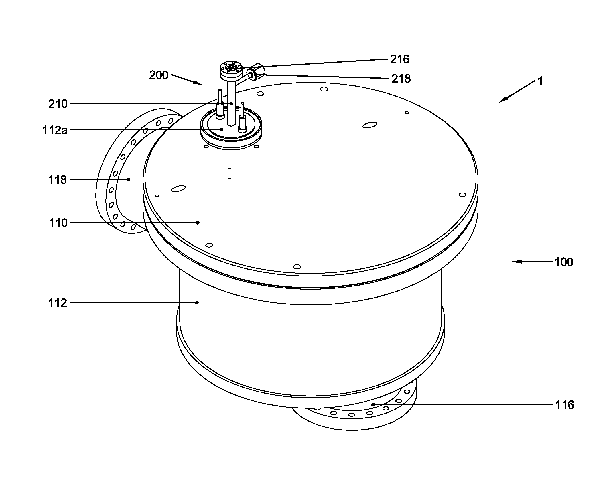
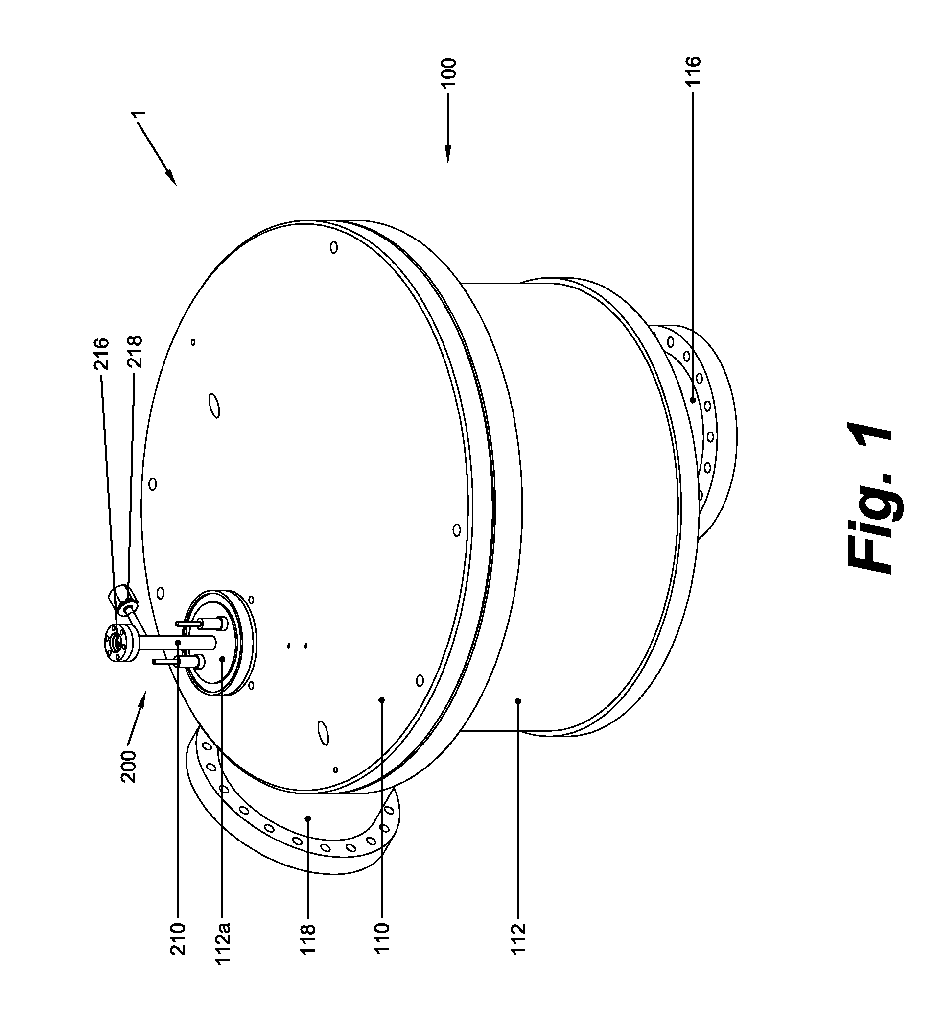
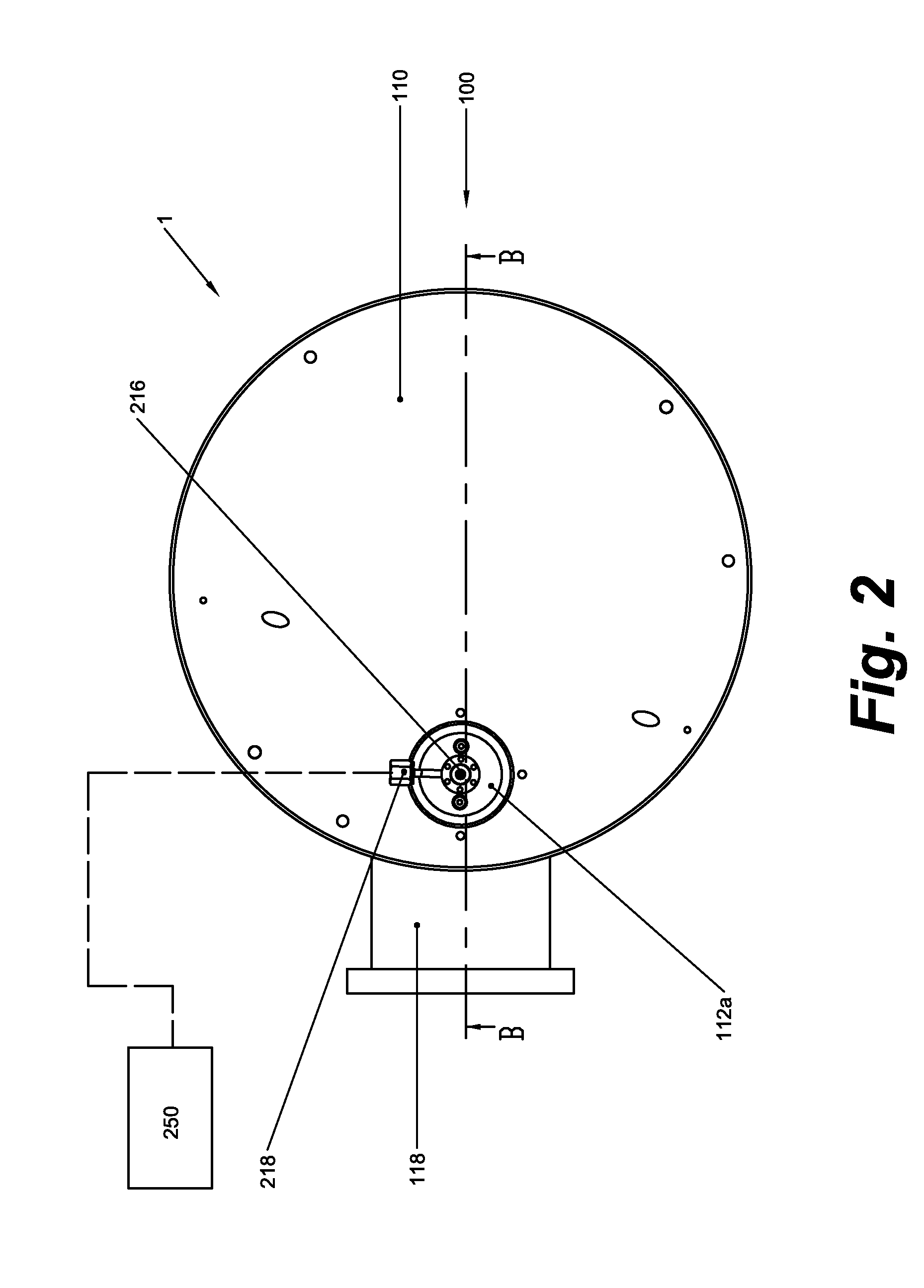
[0013]FIGS. 1-4 schematically illustrate in a perspective view, a top view and a cross-sectional side view, and a detailed / enlarged cross-sectional side view, respectively, an exemplary embodiment of a semiconductor processing apparatus 1 according to the present invention. The embodiment of the semiconductor processing apparatus 1 shown in FIG. 1 concerns a single-substrate reactor, but it is contemplated that alternative embodiments may be multi-substrate / batch reactors or furnaces, capable of processing a plurality of substrates at a time. Referring now to FIGS. 1-4.

[0014]The semiconductor processing apparatus 1 may include a reactor 100, comprising an outer reactor 110 that accommodates an inner reactor 150. The outer reactor 110 may include an outer wall 112 that defines an outer reactor chamber 114. The outer reactor 114 chamber may be coupled to a substrate handling station of a cluster tool (not shown) via a substrate transport passage 118, so as to enable the transfer of su...


PUM

PropertyMeasurementUnit
Temperatureaaaaaaaaaa

Abstract

A semiconductor processing apparatus (1), comprising: a substrate processing chamber (158), defining a substrate support location (156) at which a generally planar semiconductor substrate (300) is supportable; and at least one free radical source (200), including: a precursor gas source (250); an electric resistance heating filament (244); a sleeve (220) with a central sleeve axis (L), wherein said sleeve defines a reaction space (222) that accommodates the heating filament (244), and wherein said sleeve includes an inlet opening (224) via which the reaction space is fluidly connected to the precursor gas source (250), and an outlet opening (228) via which the reaction space is fluidly connected to the substrate processing chamber (158), said inlet and outlet openings (224, 228) being spaced apart along the central sleeve axis (L).

Description

FIELD OF THE INVENTION[0001]The present invention relates to a semiconductor processing apparatus for processing semiconductor substrates by exposing such substrates to free radicals.BACKGROUND[0002]The processing of a semiconductor substrate, e.g. the deposition of a thin film thereon, may involve exposing the substrate to free radicals. The generation of such radicals may be effected through the use of a plasma, but this approach entails several drawbacks. For one, plasma sources may be relatively bulky. In addition, a plasma may typically produce additional and undesired particles, such as electrons, ions, and highly energetic photons, that, upon contact with the substrate, may disadvantageously affect the treatment process, e.g. by being incorporated into the film that is deposited, or by otherwise damaging it.SUMMARY OF THE INVENTION[0003]It is an object of the present invention to provide for a semiconductor processing apparatus with a compact, non-plasmatic free radical sourc...

Claims


Application Information

Patent Timeline
IPC IPC(8): H01L21/306H01L21/02
CPCH01L21/306H01L21/02104H01L21/3065C23C16/452H01L21/31116
Inventor KOVALGIN, ALEXEY Y.AARNINK, ANTONIUS A. I.
Owner ASM IP HLDG BV
Why Eureka
Try Eureka