
Compensated patch-clamp amplifier for nanopore polynucleotide sequencing and other applications

Inactive Publication Date: 2013-12-26
RGT UNIV OF CALIFORNIA
View PDF6 Cites 14 Cited by
  • Summary
  • Abstract
  • Description
  • Claims
  • Application Information

AI Technical Summary

Benefits of technology

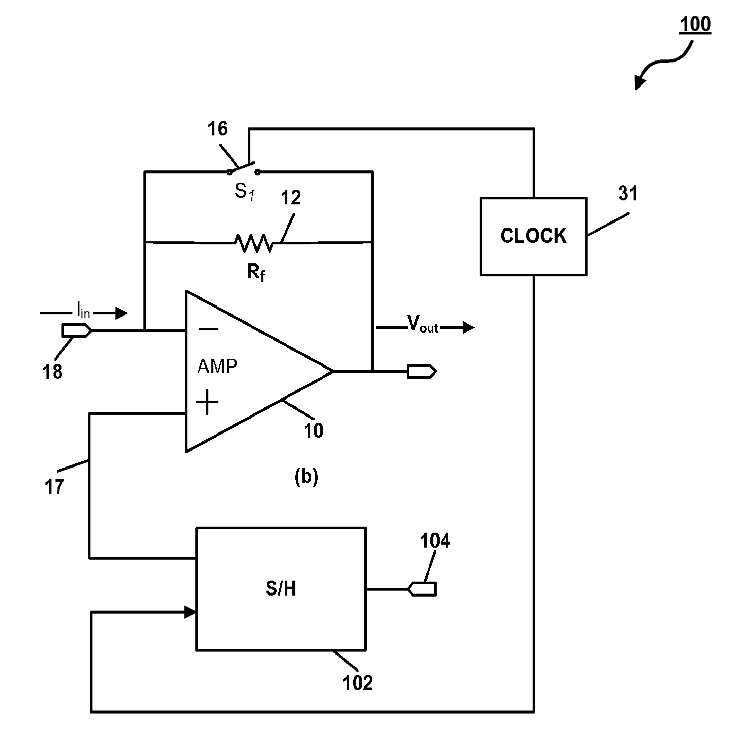
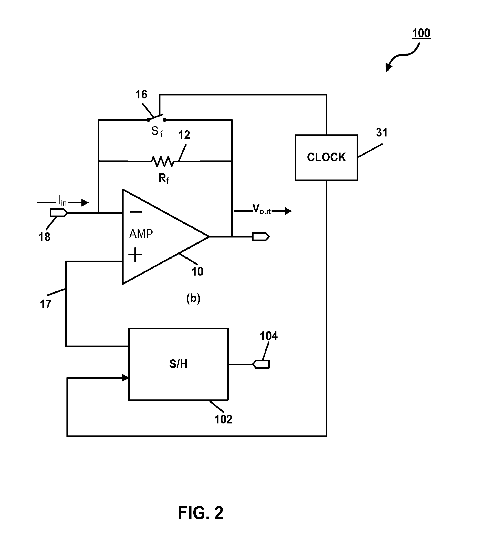
The present invention provides new, useful, and non-obvious nanopore sequcencers. These sequencers have a nanopore sensor and a patch-clamp circuit with a non-inverting input and an inverting input having a parasitic capacitance. The output is connected to the non-inverting input through an electrode series resistance. A feedback resistor is connected between the output and the inverting input. A digital-to-analog circuit receives timed digital command voltages and applies stepped command voltages to the non-inverting input in response. A reset switch selects between the output and the inverting input and closes for a time synchronized with step changes in the commanded voltage. This invention enables new methods of sequencing using nanopores and compensates for resistance to produce a predetermined voltage across the nanopore sensor.

Problems solved by technology

While the theoretical framework of nanopore sequencing is well understood, prior art nanopore sequencing systems and devices were not fully developed.
Very high gains tend to create reading instabilities caused by distributed resistances and capacitances as well as internal and external noise.
A patch-clamp must meet two very challenging design requirements.
Causes for the VOS include random process mismatches and unavoidable systematic variations.
Thus a command voltage VCMD change is time delayed due to unavoidable stray system capacitances.
Minimizing VOS and compensating for input parasitic capacitances and resistance are major design problems in nanopore sequencing.
In practice, things go wrong.
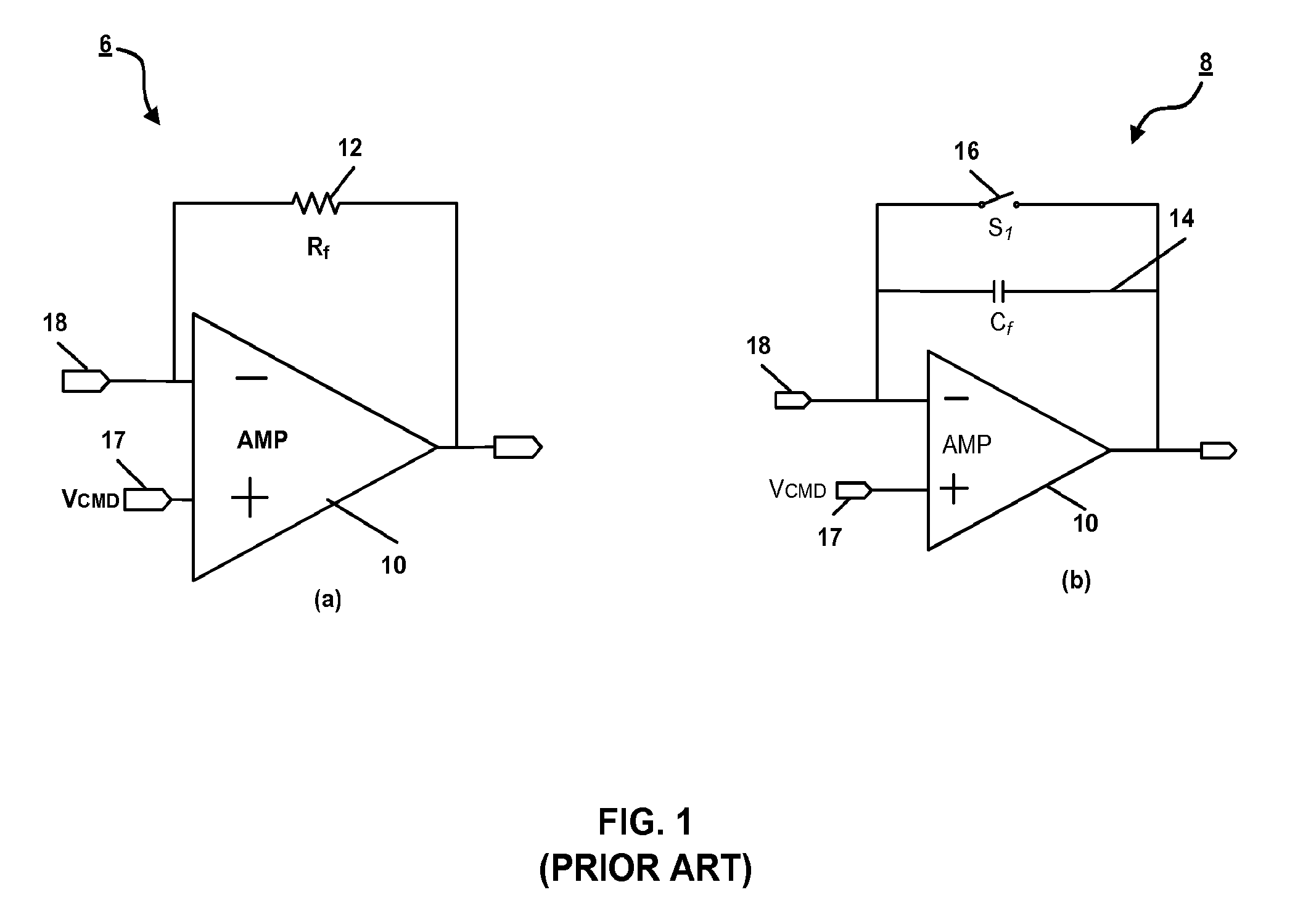
Transimpedance patch-clamp amplifiers that use resistive feedback, reference FIG. 1(a), suffer from significant time delays following command voltage VCMD changes.
That ‘dead-time’ is very undesirable.
Such prior art compensation circuitry not only increased the complexity of the basic patch-clamp but resulted in an increased input capacitance which not only limited the bandwidth of resistive feedback patch-clamp circuits, such as the resistive feedback patch-clamp circuit 6, but usually resulted in output voltageringing” in response to a step input.
The result is a much larger and more complex patch-clamp amplifier.
Prior art compensation of patch-clamp amplifiers used additional amplifiers to estimate series resistance (RS) and parasitic capacitance (CP), a rather complex circuit resulted.

Method used


Image

  • Compensated patch-clamp amplifier for nanopore polynucleotide sequencing and other applications
  • Compensated patch-clamp amplifier for nanopore polynucleotide sequencing and other applications
  • Compensated patch-clamp amplifier for nanopore polynucleotide sequencing and other applications

Examples


Embodiment Construction

[0041]The presently disclosed subject matter now will be described more fully hereinafter with reference to the accompanying drawings in which one embodiment is shown. However, it should be understood that this invention may take many different forms and thus should not be construed as being limited to the embodiment set forth herein.

[0042]All publications mentioned herein are incorporated by reference for all purposes to the extent allowable by law. In addition, in the figures like numbers refer to like elements throughout. Additionally, the terms “a” and “an” as used herein do not denote a limitation of quantity, but rather denote the presence of at least one of the referenced items.

[0043]In what follows a generic nanopore sensor 302 (reference FIG. 6) is described, used, and compensated for. It should be understood that a nanopore sensor 302 might incorporate a living cellular membrane or it might incorporate a solid-state nanopore. Furthermore, while not all circuits that are su...


PUM

PropertyMeasurementUnit
Electrical resistanceaaaaaaaaaa
Currentaaaaaaaaaa
Electrical conductoraaaaaaaaaa

Abstract

A compensated patch-clamp system for polynucleotide sequencing and other applications.

Description

RELATIONSHIP TO OTHER APPLICATIONS[0001]To the extent allowed by law this application claims priority to and the benefit of U.S. provisional patent application Ser. No. 61 / 572,829 filed 20 Jul. 2011, entitled “A SWITCHED VOLTAGE PATCH-CLAMP AMPLIFIER FOR DNA SEQUENCING ON SOLID-STATE NANOPORE”. That application and any publication cited therein are hereby incorporated by reference to the fullest extent allowed by law.STATEMENT OF SUPPORT[0002]This invention was made partly using funds from the National Science Foundation, NSF Career grant number ECCS-0845766. The US Federal Government has certain rights to this invention.FIELD OF THE INVENTION[0003]The presently disclosed subject matter is directed towards electronic devices and systems suitable for use in DNA sequencers and for detecting and quantifying individual nucleotides in a polynucleotide. More particularly, the present invention relates to compensated patch-clamp amplifiers and their use in DNA sequencing systems and method...

Claims


Application Information

Patent Timeline
IPC IPC(8): G01N33/487H03F3/45
CPCG01N33/48728H03F3/45179G01N33/48721C12Q1/6869H03F3/45076H03F2203/45116H03F2203/45336
Inventor DUNBAR, WILLIAMKIM, JUNGSUKPEDROTTI, KENNETH
Owner RGT UNIV OF CALIFORNIA
Learn More