Lithography apparatus

a technology of lithography and apparatus, applied in the field of lithography apparatus, can solve the problems of temperature-dictated expansion (i.e., the expansion caused by temperature changes) of structural and optical elements, and affect the measurement results, so as to reduce the number of sensor receptacles, the effect of space saving arrangement and minimizing the influence of temperature changes

Active Publication Date: 2013-12-26
CARL ZEISS SMT GMBH
View PDF5 Cites 4 Cited by
  • Summary
  • Abstract
  • Description
  • Claims
  • Application Information

AI Technical Summary

Benefits of technology

[0014]The detection region of the sensor can be arranged at a location of the sensor receptacle which, upon a predetermined change in the temperature, is not displaced in any direction by more than a predetermined absolute value of expansion relative to the structural element. In other words, the detection region of the sensor can therefore be arranged at a temperature-invariant point. A temperature-invariant point is a point at the surface of the sensor receptacle which, upon a uniform change in the temperature of the sensor receptacle, is not displaced relative to the structural element. As in the case mentioned above, here the predetermined temperature change value can be, for example, 10 mK, preferably 100 mK, particularly preferably 1 K, and the predetermined absolute value of displacement can be, for example, 100 nm, preferably 10 nm, particularly preferably 1 nm, and in particular preferably 0.1 nm. As a result of the arrangement of the detection region of the sensor at the temperature-invariant point, too, the influence of temperature changes on the measurement result can be minimized.
[0015]The lithography apparatus can comprise a first sensor having a first detection region for detecting a physical quantity in a first detection direction, and a second sensor having a second detection region for detecting a physical quantity in a second detection direction, wherein the first sensor is arranged in such a way that, upon a change in the temperature of the sensor receptacle, the first detection region is substantially not displaced in the detection direction relative to the structural element, and the second sensor is arranged in such a way that, upon a change in the temperature of the sensor receptacle, the second detection region is substantially not displaced in the detection direction relative to the structural element. Consequently, a lithography apparatus is provided in which two sensors are arranged on a sensor receptacle, such that a more space-saving arrangement is made possible. Furthermore, in the case of this arrangement, it is advantageous that the number of sensor receptacles can be reduced. Furthermore, the influence of temperature changes on the measurement results of both sensors is minimized.

Problems solved by technology

The individual optical elements are to be positioned as exactly as possible with regard to their orientation, since even slight deviations in the position of the optical elements can lead to an impairment of the imaged pattern, which can lead to defects in the integrated circuits produced.
One problem that arises in lithography apparatuses is the temperature-dictated expansion (i.e., the expansion caused by temperature changes) of structural and optical elements.
On account of the heat arising during operation of the exposure apparatus, temperature changes can occur at the lithography apparatus, which temperature changes lead to a thermal expansion of structural and optical elements.

Method used


Image

  • Lithography apparatus
  • Lithography apparatus
  • Lithography apparatus

Examples


first exemplary embodiment

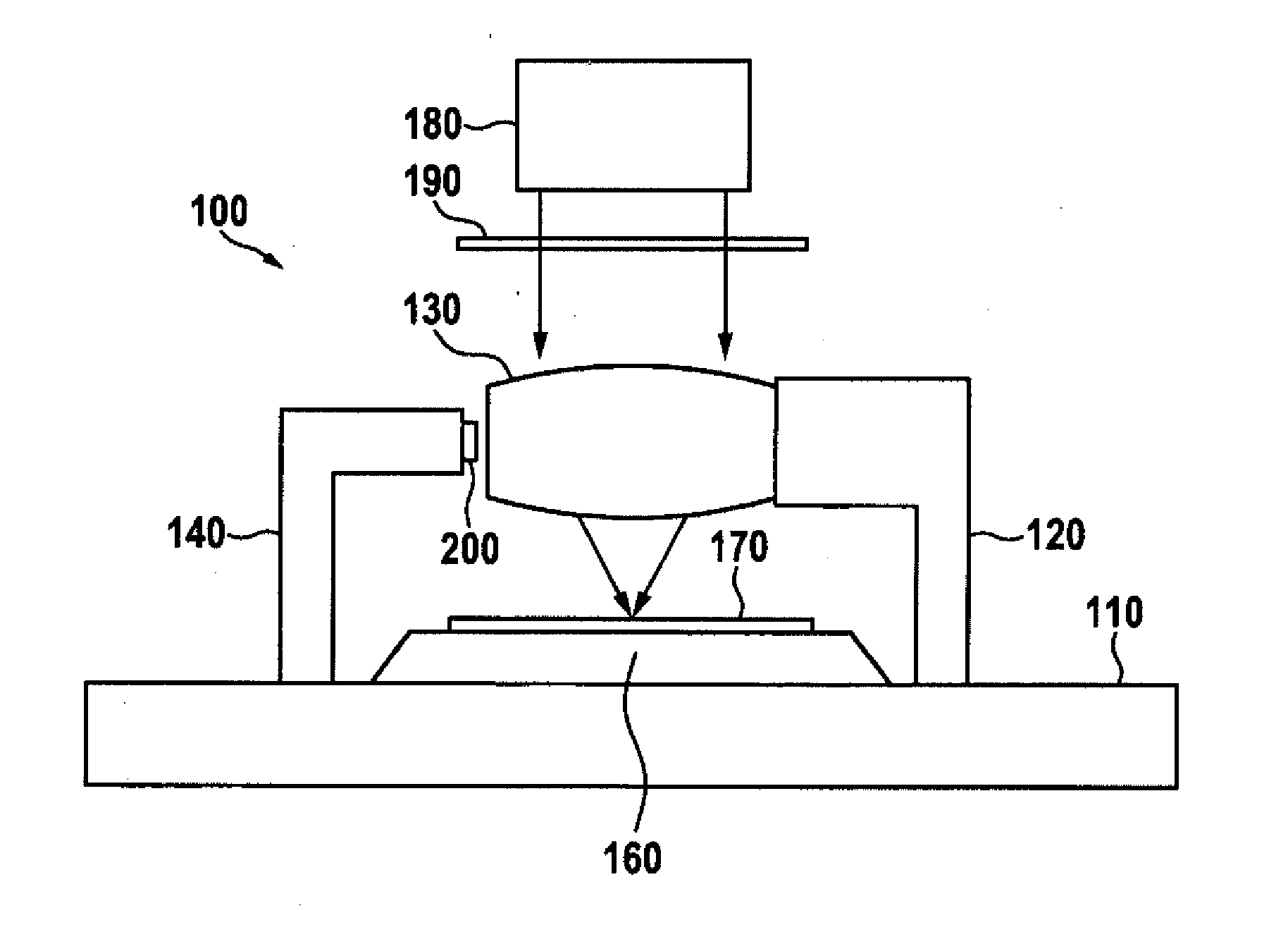
[0030]FIG. 1 shows a schematic view of a lithography apparatus 100 in accordance with a first exemplary embodiment. This lithography apparatus 100 comprises a baseplate 110, on which a holding frame 120 for mounting at least one optical element 130 and a measuring frame 140 for mounting a sensor arrangement 200 are provided. The lithography apparatus 100 typically comprises a plurality of optical elements. In FIG. 1, however, only one optical element 130 is illustrated by way of example, in order to schematically elucidate the functioning of the lithography apparatus 100.

[0031]In the example illustrated, a wafer receptacle (wafer holder) 160 is provided below the optical element 130, in which wafer receptacle a wafer 170, e.g. a silicon wafer, can be received. The wafer receptacle 160 can be embodied as a step-and-scan system, for example, which moves the wafer 170 during the exposure and also in the exposure pauses step-by-step relative to the baseplate 110.

[0032]The optical elemen...

second exemplary embodiment

[0058]FIG. 6 shows a plan view of a sensor arrangement 200 of a lithography apparatus in accordance with a second exemplary embodiment. Elements which are structurally or functionally identical to elements of the first exemplary embodiment are identified by the same reference signs and are not explained in greater detail below. In particular, the sensor arrangement 200 shown in FIG. 6 can be used as a position sensor in the lithography apparatus 100 in FIG. 1.

[0059]In this exemplary embodiment, a sensor 250 is arranged in the sensor receptacle 210, which sensor determines the position of the optical element 130 with respect to two degrees of freedom. The sensor 250 determines the position of the optical element 130 with respect to the x-direction and the y-direction relative to the measuring frame 140. The sensor 250 therefore has two detection directions in which the sensor detects a change in the position of the optical element 130. In this exemplary embodiment, too, the sensor 25...

third exemplary embodiment

[0063]FIG. 7 shows a plan view of a sensor arrangement 200 of a lithography apparatus in accordance with a third exemplary embodiment. Elements which are structurally or functionally identical to elements of the first exemplary embodiment are identified by the same reference signs and are not explained in greater detail below. In particular, the sensor arrangement 200 shown in FIG. 7 can be used as a position sensor for detecting the position of the optical element 130 in the lithography apparatus 100 in FIG. 1.

[0064]In this exemplary embodiment, two sensors 220a and 220b are arranged on the sensor receptacle 210. The sensors 220a and 220b respectively have a detection region 225a and 225b for detecting a physical quantity. In this exemplary embodiment, the sensors 220a and 220b can respectively be structurally identical to the sensor 220 from the first exemplary embodiment, and can consequently likewise in each case have an array of photodiodes arranged along a detection direction ...


PUM

PropertyMeasurementUnit
angleaaaaaaaaaa
angleaaaaaaaaaa
angleaaaaaaaaaa

Abstract

A lithography apparatus comprises a structural element, a sensor having a detection region for detecting a physical quantity in at least one detection direction with respect to the structural element, and a sensor receptacle for mounting the sensor to the structural element, wherein the sensor is arranged in such a way that the maximum displacement of the detection region in the detection direction relative to the structural element is not greater than the maximum displacement of the detection region in the detection direction in the case of an arrangement of the sensor orthogonally with respect thereto.

Description

CROSS-REFERENCE TO RELATED APPLICATIONS[0001]This application is based upon and claims the benefit of priority from the prior German Patent Application No. 10 2011 055 885.0, filed on Mar. 22, 2011, the entire contents of which are incorporated herein by reference.FIELD OF THE INVENTION[0002]The invention relates to a lithography apparatus comprising a sensor mounted with the aid of a sensor receptacle on a structural element of the lithography apparatus.RELATED ART[0003]Such a lithography apparatus is used, for example, during the production of integrated circuits or ICs in order to image a mask pattern in a mask on a substrate such as e.g. a silicon wafer. In this case, by way of example, a light beam generated by an illumination apparatus is directed through the mask onto the substrate. An exposure lens which can consist of a plurality of optical elements, such as e.g. mirrors and / or lens elements, is provided for focusing the light beam on the substrate. The individual optical e...

Claims


Application Information

Patent Timeline
Patent Type & Authority Applications(United States)
IPC IPC(8): G01N25/16
CPCG01N25/16G03F7/70825G03F7/7085G03F7/70858
Inventor LAUFER, TIMO
Owner CARL ZEISS SMT GMBH
Why Eureka
Try Eureka