Check patentability & draft patents in minutes with Patsnap Eureka AI!

Semiconductor circuit pattern measuring apparatus and method

a circuit pattern and measuring apparatus technology, applied in the direction of instruments, image analysis, image enhancement, etc., can solve the problems of unstable signal value being a reference, large deviation of product yield rate, and extremely small error permissible in manufacturing control, so as to reduce the extraction error of contours of circuit patterns and reduce the influence of product yield ra

Active Publication Date: 2014-01-02
HITACHI HIGH-TECH CORP
View PDF1 Cites 8 Cited by
  • Summary
  • Abstract
  • Description
  • Claims
  • Application Information

AI Technical Summary

Benefits of technology

The semiconductor circuit pattern measuring apparatus can improve the accuracy of measuring the shape of a circuit pattern in a photo image and reduce the impact on the yield rate of products.

Problems solved by technology

Through miniaturization in a circuit pattern accompanying by progress of recent exposure technique, an error permissible in manufacturing control is extremely small.
Further, here is a situation in which a slight measurement error largely changes a yield rate of products.
However, in a technology disclosed in JP-A-2001-338304, since a maximum intensity signal is used as a reference, a signal value being a reference tends to be unstable owing to various noises contained in images.
An erroneous selection of an intensity peak of the maximum intensity signal is in danger of staggering the extraction of contours in a photographic image of a circuit pattern, enlarging an error as a result, and reducing measurement reproducibility.
Since being extremely sensitive to errors due to miniaturization of circuit patterns at present, conventional technologies including the threshold method are in danger of failing to extract contours with sufficient accuracy, and largely changing the yield rate of products.

Method used


Image

  • Semiconductor circuit pattern measuring apparatus and method
  • Semiconductor circuit pattern measuring apparatus and method
  • Semiconductor circuit pattern measuring apparatus and method

Examples


Embodiment Construction

[0029]Next, an embodiment for performing the invention (hereinafter, referred to as an embodiment) will be accordingly described in detail with reference to the accompanying drawings.

[0030]First, a technology which is an assumption of the present embodiment will be described with reference to FIGS. 1 to 3.

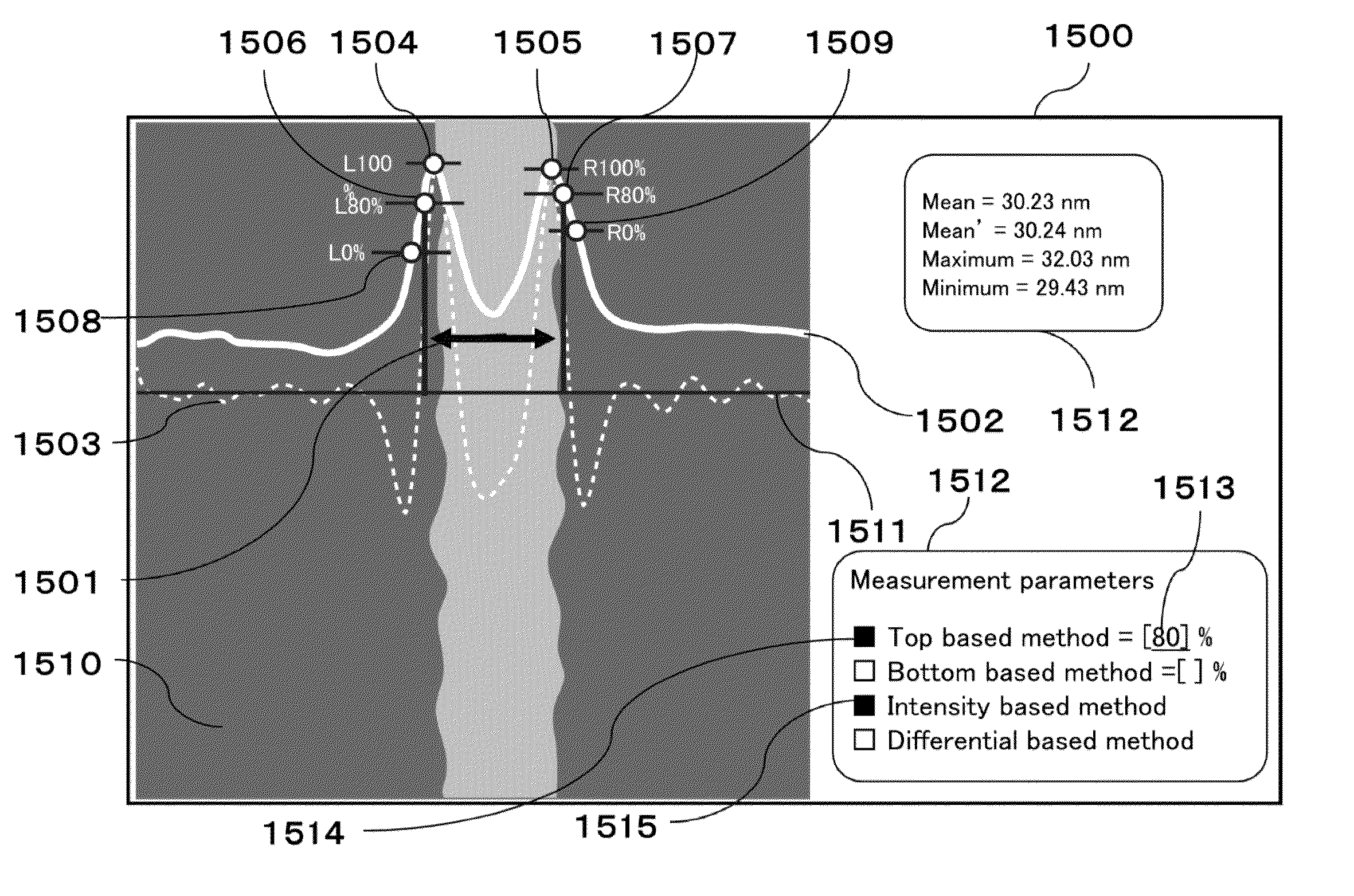
[0031]FIGS. 1A to 1E illustrate an example of a circuit pattern such as microscopic wiring and holes formed on a semiconductor wafer. FIG. 1A illustrates a line width 102 of a line 101, FIG. 1B illustrates an inter-line width 105 between lines 103 and 104, FIG. 1C illustrates a width 107 between a line 106 and a line edge 108, FIG. 1D illustrates a width 110 between line edges 109 and 111, and FIG. 1E illustrates a span 112 of a hole 113, respectively.

[0032]By using an SEM (scanning electron microscope), for example, semiconductor devices are photographed and images are analyzed as in FIGS. 1A˜1E. The above process permits sizes of circuit patterns such as wiring and holes, namely,...


PUM


Abstract

Included is a multiple resolution image generating unit which applies a plurality of noise removing filters to a semiconductor circuit pattern image and generates a multiple resolution image, a multiple resolution differential image generating unit which generates a multiple resolution differential image from a difference of images between hierarchies of the multiple resolution image, and a contour extracting unit which extracts a contour of the semiconductor circuit pattern based on an intensity signal of the semiconductor circuit pattern image. The contour extracting unit calculates an intensity signal level upon extracting a contour of the semiconductor circuit pattern from the multiple resolution image by using an image signal of the multiple resolution differential image, and extracts a contour of the semiconductor circuit pattern based on the calculated intensity signal level.

Description

INCORPORATION BY REFERENCE[0001]The present application claims priority from Japanese application JP2012-102042 filed on Apr. 27, 2012, the content of which is hereby incorporated by reference into this application.BACKGROUND OF THE INVENTION[0002]The present invention relates to a semiconductor circuit pattern measuring apparatus and a method, and particularly, to an analysis technique of images of semiconductor devices.[0003]In a manufacturing process of a semiconductor device, a size of a circuit pattern such as fine wiring and holes formed on a semiconductor wafer is measured to thereby perform manufacturing control. Contours in a photographic image of the circuit pattern are extracted so as to measure the size of the circuit pattern.[0004]In JP-A-2001-338304, a method called a threshold method is illustrated as a method for extracting contours of a circuit pattern in a photographic image. In this threshold method, by using as a reference a maximum intensity signal in a photogra...

Claims


Application Information

Patent Timeline
Patent Type & Authority Applications(United States)
IPC IPC(8): G06T7/00
CPCG06T7/0004G06T2207/30148G06T2207/20016G06T2207/20148G06T7/136
Inventor SHIBAHARA, TAKUMAOIKAWA, MICHIOSAKAI, KEIYAMAGUCHI, SATORU
Owner HITACHI HIGH-TECH CORP
Features
  • R&D
  • Intellectual Property
  • Life Sciences
  • Materials
  • Tech Scout
  • Unparalleled Data Quality
  • Higher Quality Content
  • 60% Fewer Hallucinations
Learn More