Integrated multilayer magnetoresistive sensor and manufacturing method thereof

a multi-layer magnetoresistive sensor and integrated technology, applied in the direction of magnetic field magnitude/direction, measurement devices, instruments, etc., can solve the problems of not being able to achieve optimal solution, not being able to achieve perfect orthogonality, and not being able to scale down less than 0.70.7 mm

Active Publication Date: 2014-01-16
STMICROELECTRONICS SRL
View PDF3 Cites 21 Cited by
  • Summary
  • Abstract
  • Description
  • Claims
  • Application Information

AI Technical Summary

Benefits of technology

[0031]Magnetoresistive elements are formed both in the portions oriented along X and in the portions oriented along Y so that the magnetoresistive sensor can be used as biaxial sensor. All the magnetoresistive elements are coplanar and formed during one and the same step of deposition of ferromagnetic material. Said ferromagnetic material, before definition of the magnetoresistive strip (flat film), has the easy axis oriented in a direction typically forming an angle of 45° with respect to both of the axes of sensitivity of the ferromagnetic element. The sha...

Problems solved by technology

However, the solution obtained is not optimal in so far as further steps of compensation of the signal generated by the magnetoresistive elements are desirable on account of the fact that, even though the geometrical anisotropy orients the easy axis of the magnetoresistive elements that are sensitive to the field along...

Method used


Image

  • Integrated multilayer magnetoresistive sensor and manufacturing method thereof
  • Integrated multilayer magnetoresistive sensor and manufacturing method thereof
  • Integrated multilayer magnetoresistive sensor and manufacturing method thereof

Examples


Embodiment Construction

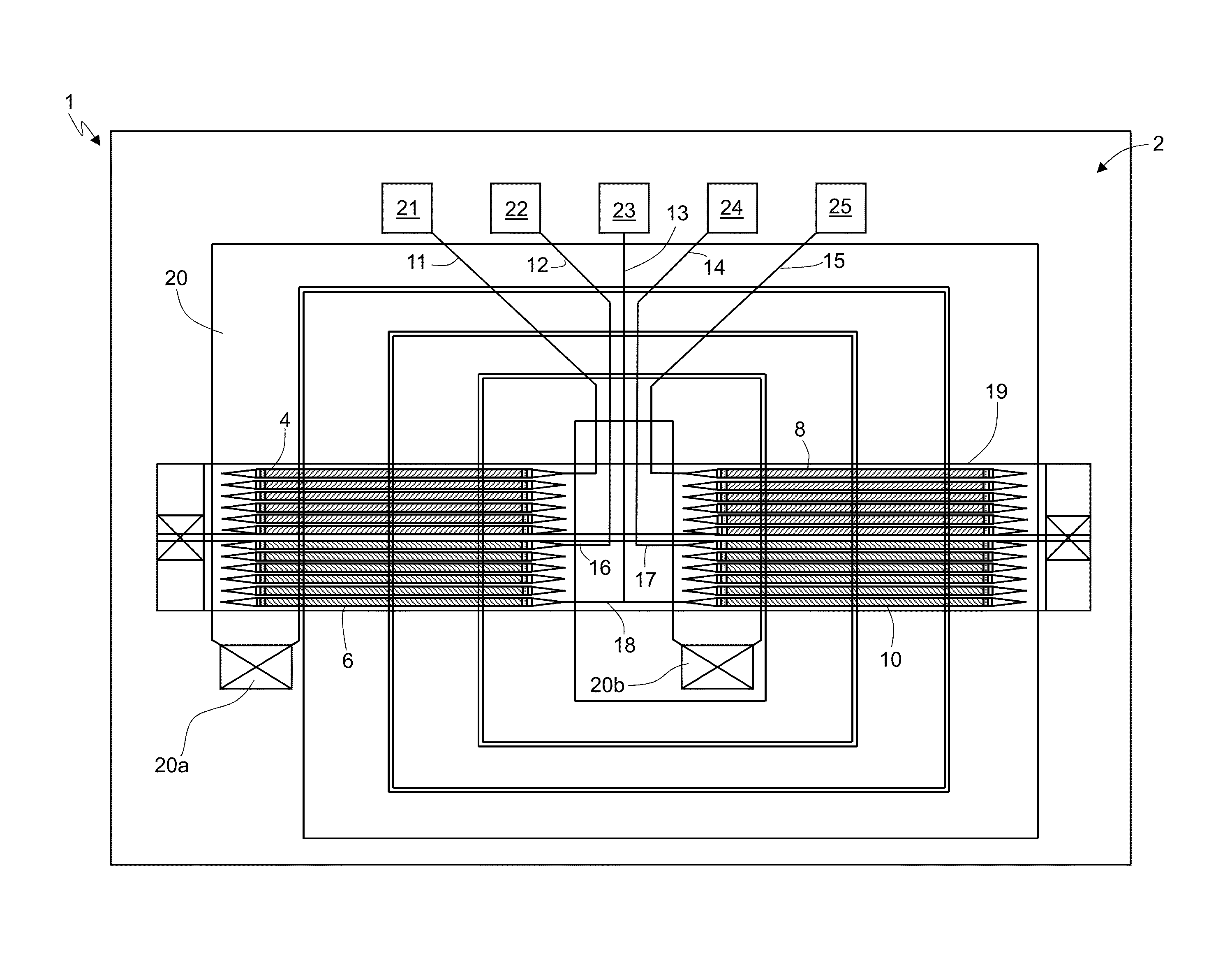
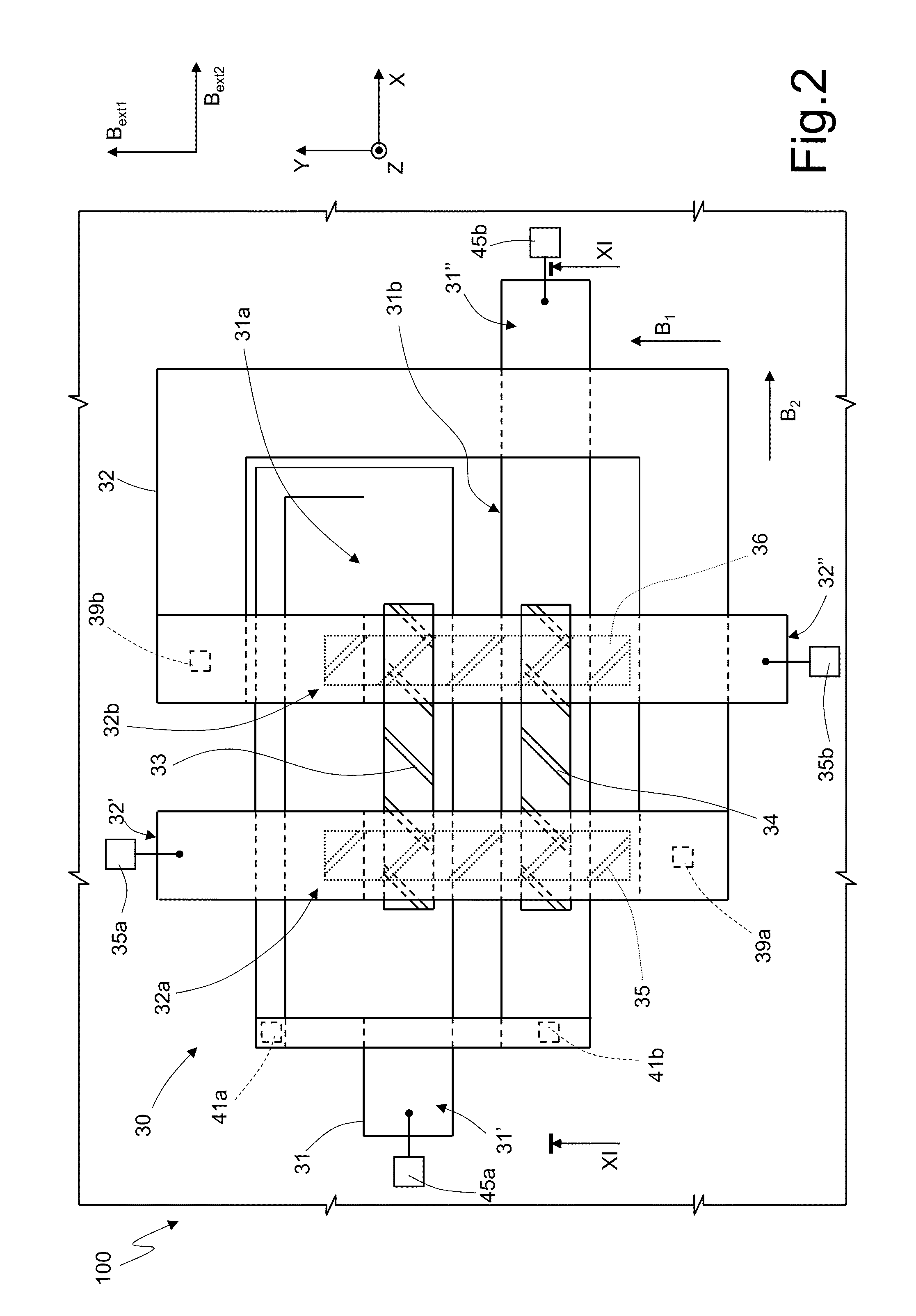
[0056]FIG. 2 shows, in top-plan view and in schematic form, a portion of a magnetic-field sensor 30 formed in a wafer 100 comprising a plurality of metal levels separated from one another by dielectric layers, according to one embodiment of the present disclosure.

[0057]The magnetic-field sensor 30 is, in particular, a two-axis sensor designed to sense external magnetic fields Bext1 and Bext2 acting in two mutually perpendicular directions (in particular, in the representation of FIG. 2, along the axes Y and X, respectively).

[0058]The magnetic-field sensor 30 comprises a first magnetic-field generator 31 and a second magnetic-field generator 32. The first magnetic-field generator 31 is formed by planar conductive strips extending in a plurality of metal levels, as described more fully hereinafter, for example, with reference to FIGS. 3 and 4. The second magnetic-field generator 32 is also formed by planar conductive strips extending in a plurality of metal levels at least in part dif...


PUM

PropertyMeasurementUnit
Magnetic fieldaaaaaaaaaa
Areaaaaaaaaaaa
Distanceaaaaaaaaaa

Abstract

A magnetic-field sensor includes: a chip including a substrate having a first surface and an insulating layer covering the first surface; first and second magnetoresistors each extending into the insulating layer and having a main axis of magnetization and a secondary axis of magnetization; a first magnetic-field generator configured to generate a first magnetic field having field lines along the main axis of magnetization of the first magnetoresistor; a second magnetic-field generator configured to generate a second magnetic field having field lines along the main axis of magnetization of the second magnetoresistor. The main axes of magnetization extending transversely to each other and the secondary axes of magnetization extending transversely to each other. The first and second magnetoresistors extend into the insulating layer at a first distance and a second distance, respectively, that differ from one another, from the first surface.

Description

BACKGROUND[0001]1. Technical Field[0002]The present disclosure relates to an integrated multilayer magnetoresistive sensor and to the manufacturing method thereof, more in particular to a magnetic-field sensor comprising anisotropic magnetoresistive elements.[0003]2. Description of the Related Art[0004]Magnetic-field sensors of an AMR (anisotropic magnetoresistance) type are used in a plurality of applications and systems, for example, in compasses, in systems for detecting ferromagnetic materials, in the detection of currents and in a wide range of other applications, thanks to their capacity for detecting natural magnetic fields (for example, the Earth's magnetic field) and magnetic fields generated by electrical components (such as electrical or electronic devices and lines traversed by electric current).[0005]In a known way, the phenomenon of anisotropic magnetoresistivity occurs within particular ferromagnetic materials, which, when subjected to an external magnetic field, unde...

Claims


Application Information

Patent Timeline
IPC IPC(8): G01R33/09
CPCG01R33/096G01R33/0017G01R33/0206Y10T29/49034Y10T29/49043Y10T29/49044G01R33/0052G01R33/09
Inventor PACI, DARIOZERBINI, SARAHVIGNA, BENEDETTO
Owner STMICROELECTRONICS SRL
Why Eureka
Try Eureka