Vacuum sealed package, printed circuit board having vacuum sealed package, electronic device, and method for manufacturing vacuum sealed package

a technology of printed circuit boards and sealed packages, which is applied in the direction of electrical apparatus casings/cabinets/drawers, optical radiation measurement, hermetically sealed casings, etc., can solve the problems of sensitivity drop, decrease in the performance of electronic devices, etc., and achieve simple system, improve package productivity, and reduce melting point

Inactive Publication Date: 2014-01-23
NEC CORP
View PDF1 Cites 23 Cited by
  • Summary
  • Abstract
  • Description
  • Claims
  • Application Information

AI Technical Summary

Benefits of technology

[0031]According to the present invention, since the third conductor pad is positioned outside of the hollow portion of the package main body portion and is connected via a thermally conductive material with the first conductor pad that is formed on the wiring substrate that is positioned in the hollow portion of the package main body portion, after evacuating and sealing the hollow portion of the package main body portion, if for example a laser beam or the like is emitted onto the third conductor pad, the first conductor pad and a getter material on the first conductor pad are heated via the thermally conductive material. Thereby, it is possible to cause gas molecules in the hollow portion of the package main body portion to adsorb to the getter material. That is, in the present invention, after evacuating and sealing the hollow portion of the package main body portion, it is possible to heat the getter material on the first conductor pad in the hollow portion of the package main body portion via the thermally conductive material. Accordingly, in a package employing a system in which sealing of the package main body portion is performed in a state of the interior being evacuated in advance, it is possible to maintain the vacuum state after sealing of the package main body portion, and possible to significantly improve the productivity of the package with a simple system.
[0032]Also, in the present invention, since the sealing member that seals the through-hole with the inside and outside of the hollow portion of the package main body portion is constituted by partially heating the vicinity of the through-hole, and the constituent material of the package main body portion being melted, for example by making the sealing member a material with a lower melting point than the package main body portion, it is possible to perform sealing of the through-hole with a low-power laser device, and as a result it is possible to lower the manufacturing cost.
[0033]Also, in an exemplary embodiment of the present invention, the low-melting-point portion that includes a low-melting-point metal material with a lower melting point than the package main body portion is provided in the vicinity of the through-hole, and the sealing member is formed that plugs the through-hole by heating and melting the low-melting-point portion. In a conventional structure, since there is no low-melting-point metal film in the interior of the through-hole, and the main material itself of the package main body portion is exposed, a wetting defect occurs, and so more time is required in the case of plugging the interior of the through-hole. In contrast, in the exemplary embodiment of the present invention, by heating the low-melting-point portion, the low-melting-point portion wetly spreads well in the interior of the through-hole, and so there is the advantage of being able to reliably plug the through-hole. That is, in a package employing a system in which sealing of the package main body portion is performed in a state of the interior being evacuated in advance, it is possible to perform sealing of the package main body portion, and possible to significantly improve the productivity of the package with a simple system.

Problems solved by technology

As a result, the problem arises of the performance of the electronic device decreasing (for example, in an infrared ray sensor, the sensitivity of the output signal drops).
However, when left in the atmosphere, gas molecules end up being adsorbed on the surface thereof, resulting in a saturated state in which the no more gas can be adsorbed.

Method used


Image

  • Vacuum sealed package, printed circuit board having vacuum sealed package, electronic device, and method for manufacturing vacuum sealed package
  • Vacuum sealed package, printed circuit board having vacuum sealed package, electronic device, and method for manufacturing vacuum sealed package
  • Vacuum sealed package, printed circuit board having vacuum sealed package, electronic device, and method for manufacturing vacuum sealed package

Examples


exemplary embodiment 1

[0105]Hereinbelow, a vacuum sealed package in a first exemplary embodiment of the present invention shall be described with reference to FIG. 1 to FIG. 4.

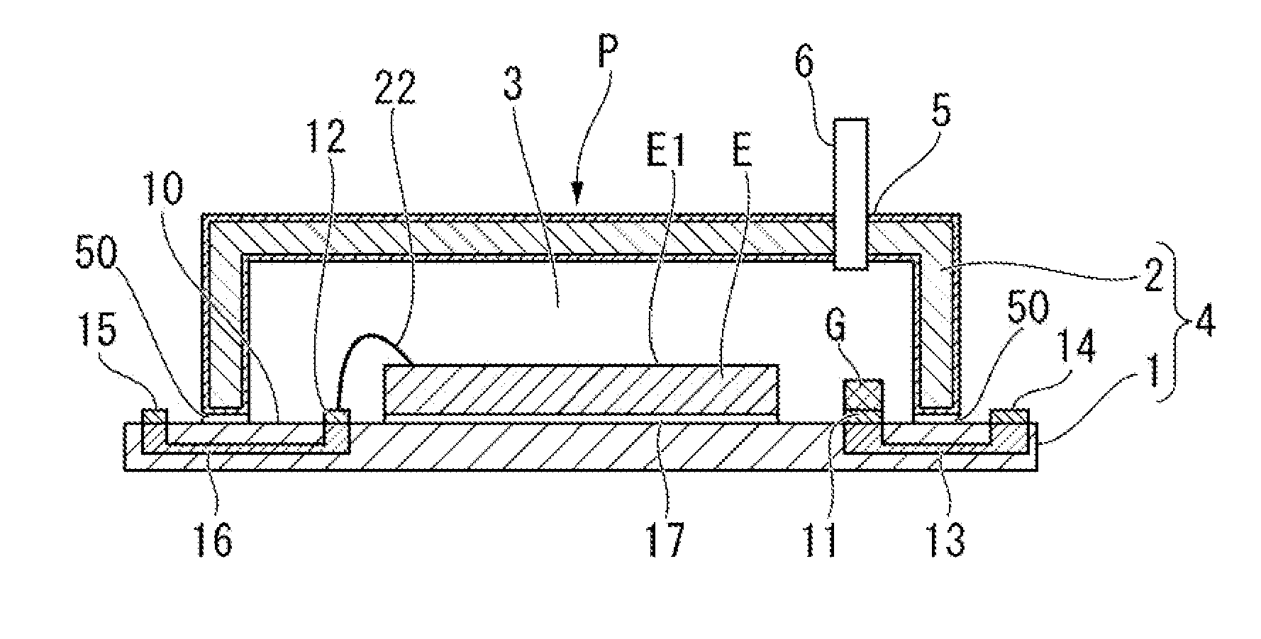
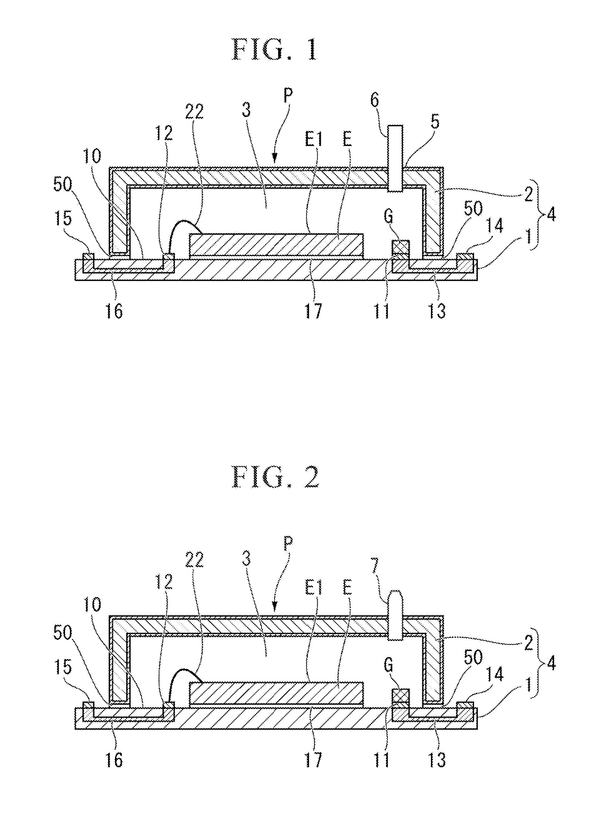
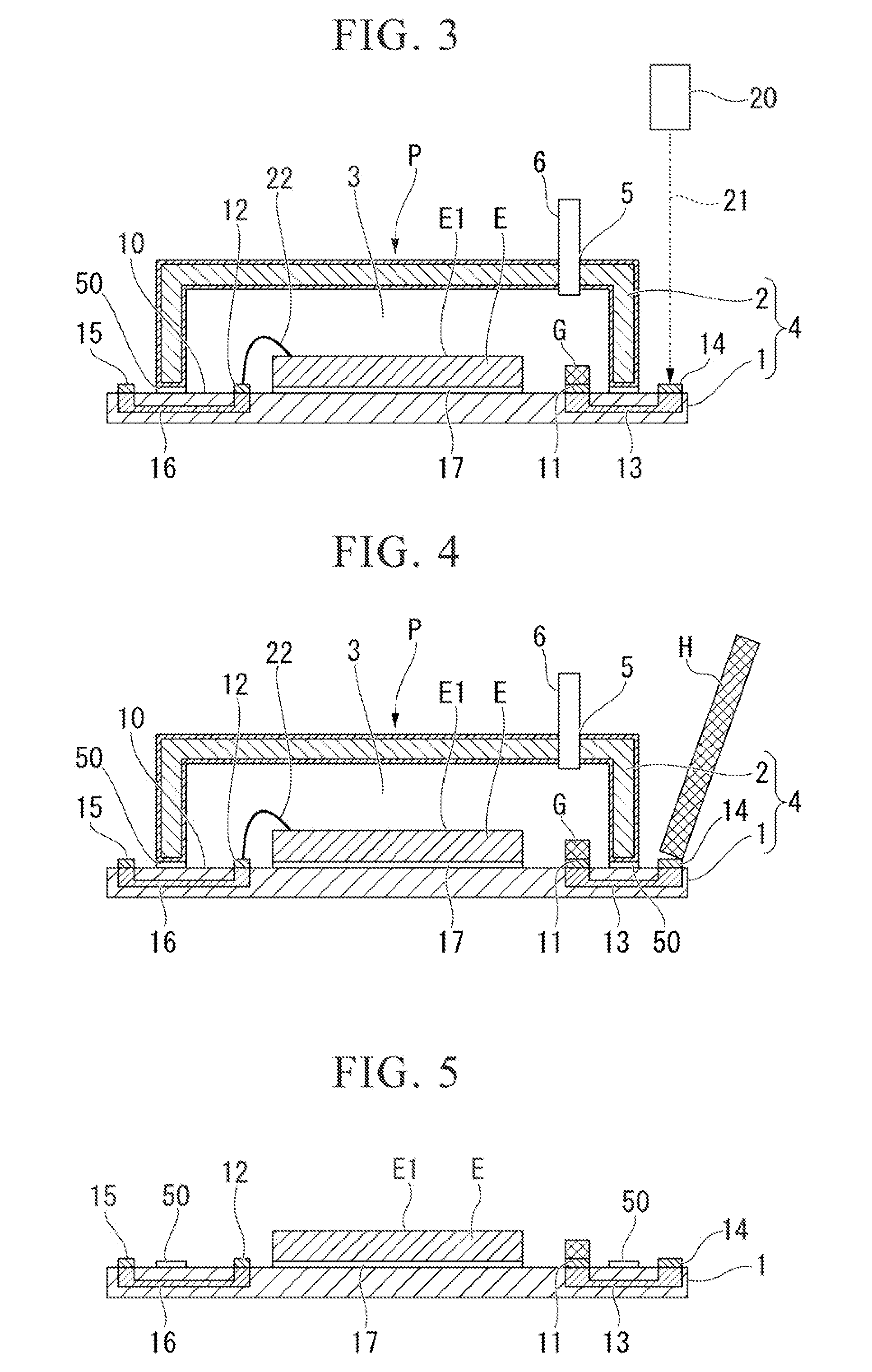
[0106]First, in these figures, FIG. 1 is a cross-sectional view that shows the state in which the inside of a package that has been evacuated by an exhaust tube. FIG. 2 is a cross-sectional view that shows the sealed state of a package that has been evacuated.

[0107]In these figures, a vacuum sealed package P includes a package main body portion 4 in which a first main body portion 1 with a wiring substrate 10 (described below) integrated on the upper surface thereof and a second main body portion 2 that serves as a lid member are joined with a hollow portion 3 interposed therebetween, and a getter material G and an electronic device E that are provided in the hollow portion 3 within this package main body portion 4.

[0108]A through-hole 5 that brings the hollow portion 3 and the outside of the package main body 4 into communication ...

exemplary embodiment 2

[0148]Next, a second exemplary embodiment of the present invention shall be described with reference to FIG. 15 to FIG. 25. In FIG. 15 and FIG. 16, portions that are the same as the constituent elements in FIG. 1 to FIG. 14 are denoted by the same reference symbols, and so explanations thereof are omitted. Since the basic configuration of this second exemplary embodiment is the same as the first exemplary embodiment described above, only the points of difference therebetween shall mainly be described here. Note that FIG. 15 is a cross-sectional view that shows the state prior to sealing the through-hole 5, while FIG. 16 is a cross-sectional view that shows the state after sealing the through-hole 5.

[0149]In this second exemplary embodiment, the through-hole 5 for evacuation is formed in advance in the second main body portion 2 that serves as the lid member of the package main body portion 4. The method of plugging this through-hole 5 differs from the first exemplary embodiment. The...

exemplary embodiment 3

[0195]Next, a third exemplary embodiment shall be described with reference to FIG. 26A to FIG. 28. In these figures, the same reference symbols are given to those portions that are the same as the constituent elements in the preceding FIG. 1 to FIG. 25, and descriptions thereof are omitted. Hereinbelow, only the points of difference with the aforementioned exemplary embodiments shall be described. Note that FIG. 26A of the third exemplary embodiment is an example of the first conductor pad 11 and the second conductor pad 12 being provided at opposing positions sandwiching the electronic device E, and FIG. 26B is an example of the first conductor pad 11 and the second conductor pad 12 being provided at positions adjacent to the side positions of the electronic device E.

[0196]A width 51 of a conductor pattern 50 that surrounds the periphery of an electronic device E that is formed on the wiring substrate 10, which is a characteristic of the third exemplary embodiment of the present in...


PUM


Abstract

A vacuum sealed package includes a package main body portion in which a first main body portion and a second main body portion are bonded via a hollow portion, and a getter material and an electronic device that are provided within the hollow portion, and in the state of the hollow portion being evacuated via a through-hole that brings the inside and the outside of the hollow portion into communication, the package main body portion is sealed with a sealing member, the getter material and the electronic device are connected to a first conductor pad and a second conductor pad, the first conductor pad is connected with a third conductor pad via a thermally conductive material, and the second conductor pad is electrically connected with a fourth conductor pad on a wiring substrate.

Description

[0001]This present application is a Divisional application of Ser. 13 / 148,524 filed on Aug. 9, 2011, which is a National Stage Entry of international application PCT / JP2010 / 000451, filed on Jan. 27, 2010, which claims the benefit of priority from Japanese Patent Application 2009-036511, filed on Feb. 19, 2009, the disclosures of all of which are incorporated in their entirety by reference herein.TECHNICAL FIELD[0002]The present invention relates to a vacuum sealed package that vacuum seals an electronic device, and a method for manufacturing the vacuum sealed package.BACKGROUND ART[0003]In recent years, there has been a demand for miniaturization, increased performance, and cost reductions for packages and devices in which an electronic device such as an infrared ray sensor, gyro sensor (angular velocity sensor), temperature sensor, pressure sensor, and acceleration sensor is vacuum-encapsulated therein. In particular, in a package or device that implements an infrared ray sensor (i...

Claims


Application Information

Patent Timeline
Patent Type & Authority Applications(United States)
IPC IPC(8): H05K5/06
CPCH05K5/066G01J5/045H01L23/057H01L23/10H01L23/26H01L2924/01079H01L2924/09701H01L2224/32225H01L2224/48227H01L2224/73265H01L2924/15192H01L2924/19107H01L2224/48091H01L2924/10253H01L2924/3025H01L24/73H01L2924/14H01L2924/16151H01L2924/16152G01J5/051H01L2924/00012H01L2924/00014H01L2924/00
Inventor YAMAZAKI, TAKAOSANO, MASAHIKOKURASHINA, SEIJI
Owner NEC CORP
Why Eureka
Try Eureka