Multi level antifuse memory device and method of operating the same

Active Publication Date: 2014-01-23
SAMSUNG ELECTRONICS CO LTD
View PDF3 Cites 12 Cited by
  • Summary
  • Abstract
  • Description
  • Claims
  • Application Information

AI Technical Summary

Benefits of technology

[0032]According to an exemplary of the inventive concept, a method of operating an antifuse memory device includes: selecting a resistor from a reference resistance unit including a plurality of resistors; applying a first voltage to an antifuse memory cell including an antifuse; applying the first voltage to a reference current generation unit including the reference resistance unit and generating a reference current corresponding to the selected resistor; and comparing an intensity of a cell current flowing through the antifuse with an intensity of the reference current. The first voltage may be sufficient to cause dielectric breakdown of the antifuse. The method may further include halting application of the voltage to the antifuse memory when a result of the comparing indicates the intensity of the cell current is higher than the reference current. The selected resistor may indicate a multi-bit pattern to be programmed to the antifuse memory cell.
[0033]According to an exemplary embodiment of the inve

Problems solved by technology

However, since the method used to breakdown the dielectric substanc

Method used


Image

  • Multi level antifuse memory device and method of operating the same
  • Multi level antifuse memory device and method of operating the same
  • Multi level antifuse memory device and method of operating the same

Examples


Example

[0046]The inventive concept will now be described more fully with reference to the accompanying drawings, in which exemplary embodiments of the inventive concept are shown. It should be understood, however, that there is no intent to limit exemplary embodiments of the inventive concept to the particular forms disclosed, but conversely, exemplary embodiments of the inventive concept are to cover all modifications, equivalents, and alternatives falling within the spirit and scope of the inventive concept.

[0047]Like reference numerals denote like elements in the drawings. In the attached drawings, sizes of structures may be exaggerated for clarity. As used herein, the singular forms “a”, “an”, and “the” are intended to include the plural forms as well, unless the context clearly indicates otherwise.

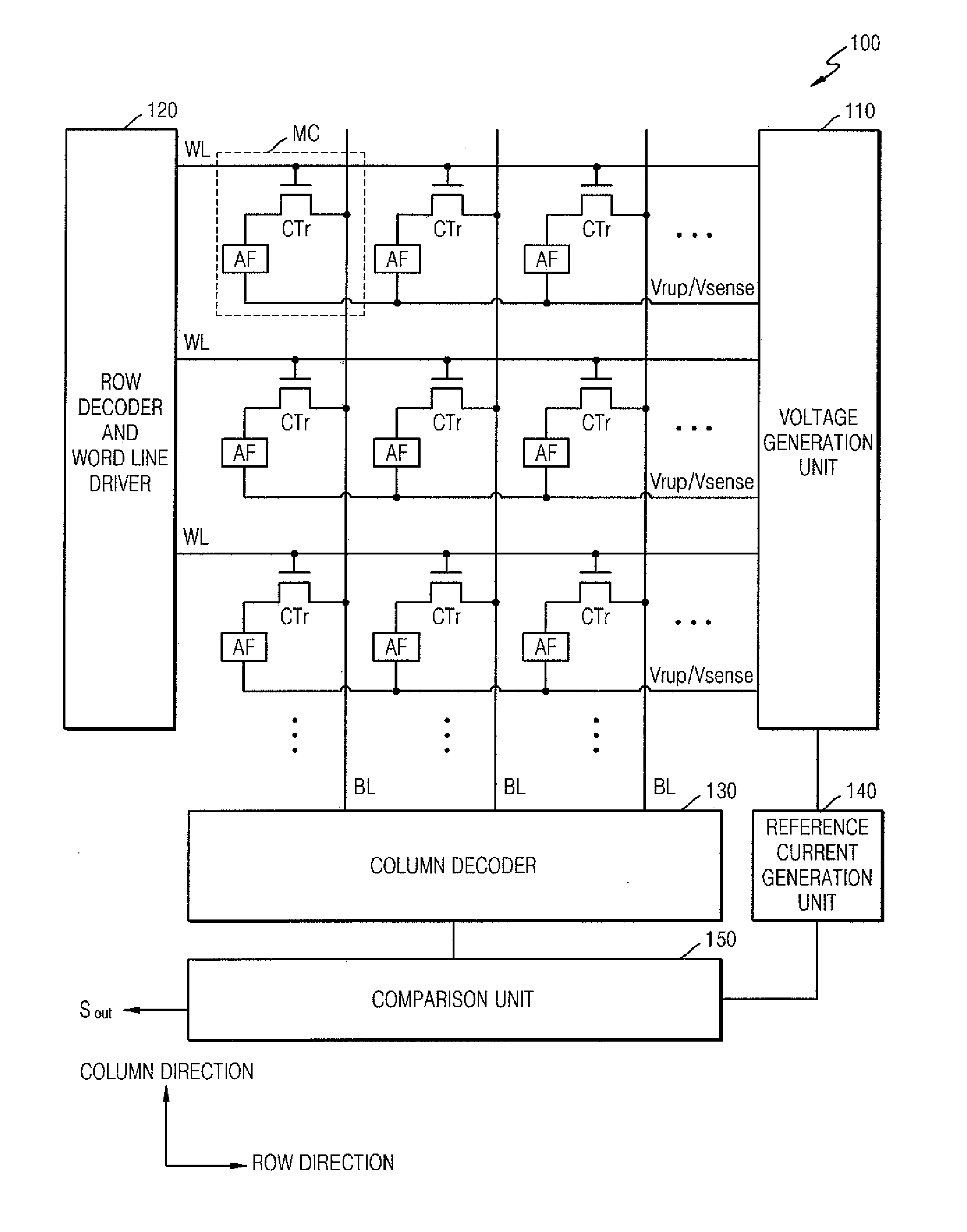
[0048]FIG. 1 is a schematic block diagram illustrating an antifuse memory device 100 according to an exemplary embodiment of the inventive concept.

[0049]Referring to FIG. 1, the antifuse mem...


PUM


Abstract

An antifuse memory device includes an antifuse memory cell, a reference current generation unit, and a comparison unit. The antifuse memory cell includes an antifuse. The reference current generation unit provides a reference current selected from a plurality of reference currents. The comparison unit compares an intensity of a cell current flowing through the antifuse with an intensity of the reference current and provides an output signal corresponding to a result of the comparison.

Description

CROSS-REFERENCE TO RELATED APPLICATIONS[0001]This application claims priority to Korean Patent Application No. 10-2012-0078955, filed on Jul. 19, 2012, in the Korean Intellectual Property Office, the disclosure of which is incorporated herein in its entirety by reference.BACKGROUND[0002]1. Technical Field[0003]The inventive concept relates to an antifuse, and more particularly, to an antifuse memory device capable of storing a plurality of bits, and a method of programming and reading the same.[0004]2. Discussion of Related Art[0005]An antifuse is an electrical device that performs a function that is opposite to that of a fuse. Whereas a fuse starts with a low resistance and is designed to break an electrically conductive path, an antifuse starts with a high resistance and is designed to create an electrically conductive path when the voltage across the antifuse exceeds a certain level. A high voltage is applied to a dielectric substance within the antifuse, which causes the dielect...

Claims


Application Information

Patent Timeline
IPC IPC(8): G11C17/16
CPCG11C17/16G11C11/5692G11C17/18G11C2211/5624G11C2211/563
Inventor JANG, MIN-SOOSEO, YOUNG-HUNLEE, CHAN-YONG
Owner SAMSUNG ELECTRONICS CO LTD
Why Eureka
Try Eureka