Light emitting device and electronic apparatus

Active Publication Date: 2014-01-30
SEIKO EPSON CORP
View PDF10 Cites 17 Cited by
  • Summary
  • Abstract
  • Description
  • Claims
  • Application Information

AI Technical Summary

Benefits of technology

[0034]According to this application example, since the light emitting device according to any one of the aforementioned application examples is

Problems solved by technology

However, as described in JP-A-08-241048 and JP-A-2008-300367, in the case where what is called an insulating layer such as a passivation layer, a flattening insulating layer, or the like covers the end portions of the positive electrode, enhancement of the aperture ratio is limited.
If there is a thinned-film portion in the functional layer, an electric current intensively flows in the thinned-film portion, whereby the light emitting element is likely to be deteriorated.
In the case where a light emitting element of a specif

Method used


Image

  • Light emitting device and electronic apparatus
  • Light emitting device and electronic apparatus
  • Light emitting device and electronic apparatus

Examples


Example

First Embodiment

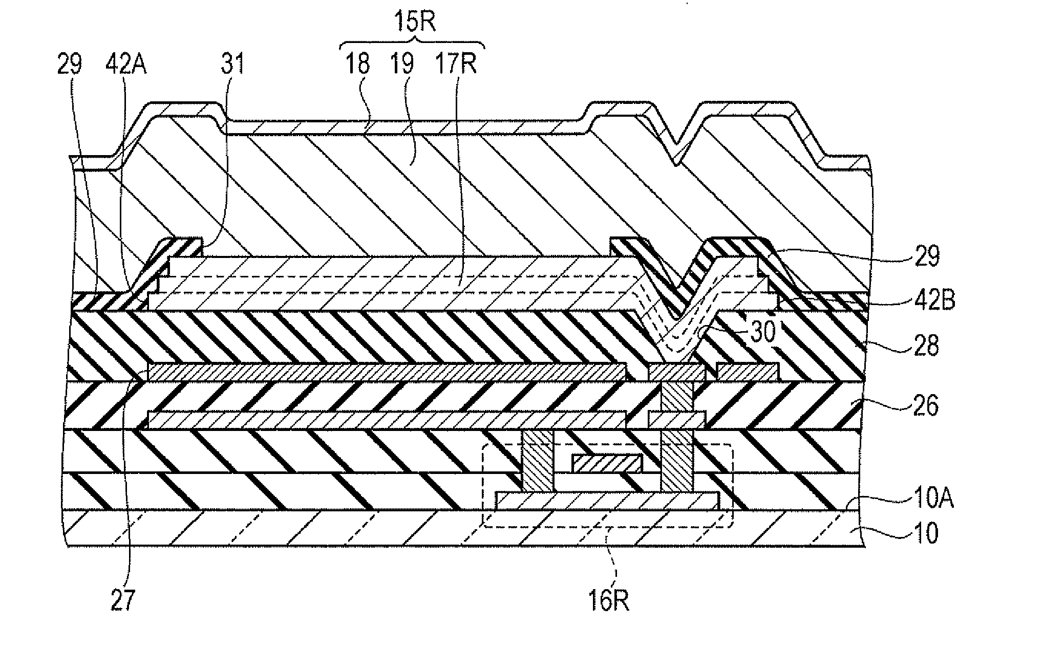
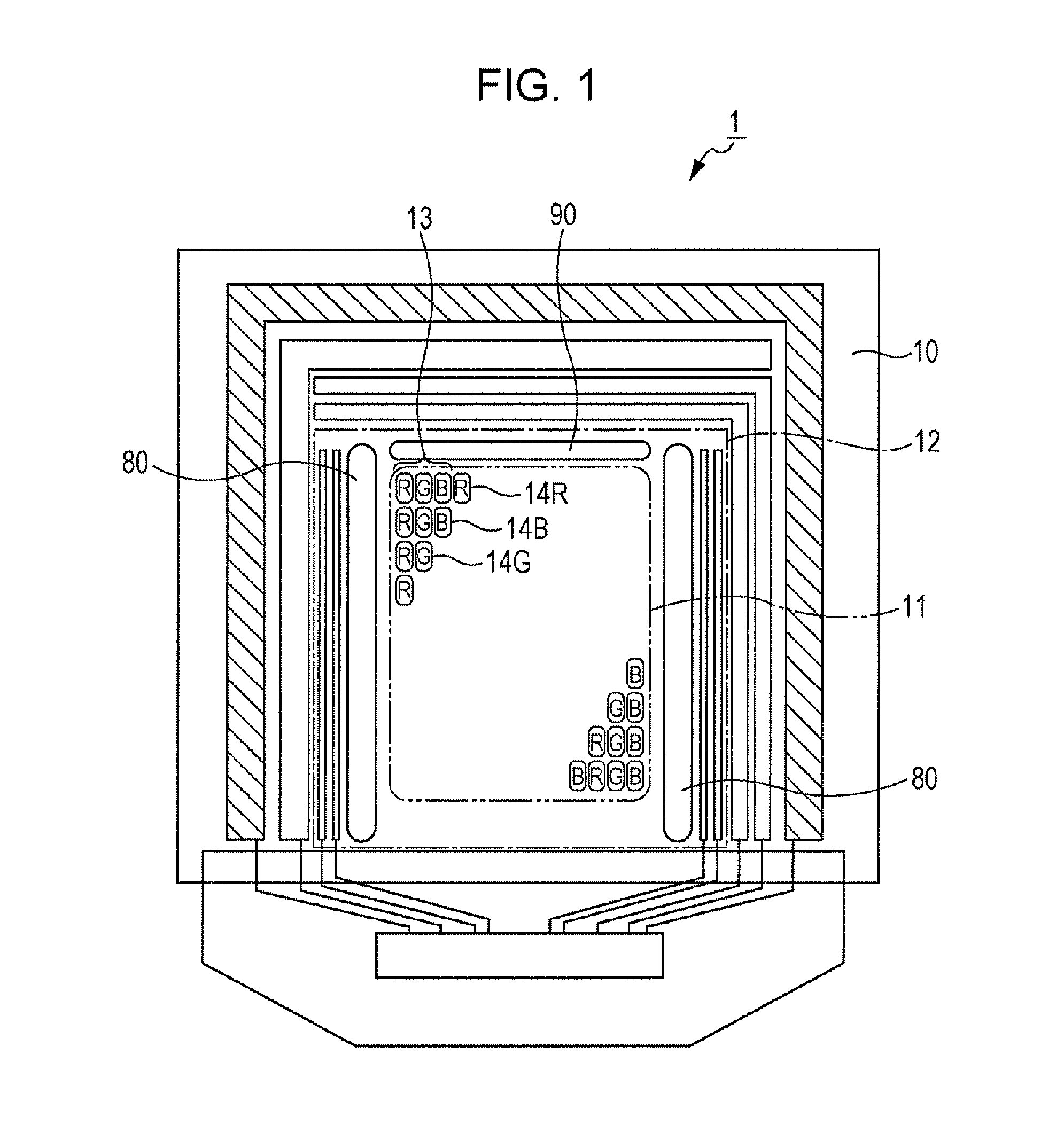
[0046]Light Emitting Device

[0047]FIG. 1 is a schematic plan view illustrating a basic configuration of a light emitting device according to a first embodiment.

[0048]First, the schematic configuration of an organic electroluminescence (EL) device 1 as the light emitting device according to the first embodiment will be described.

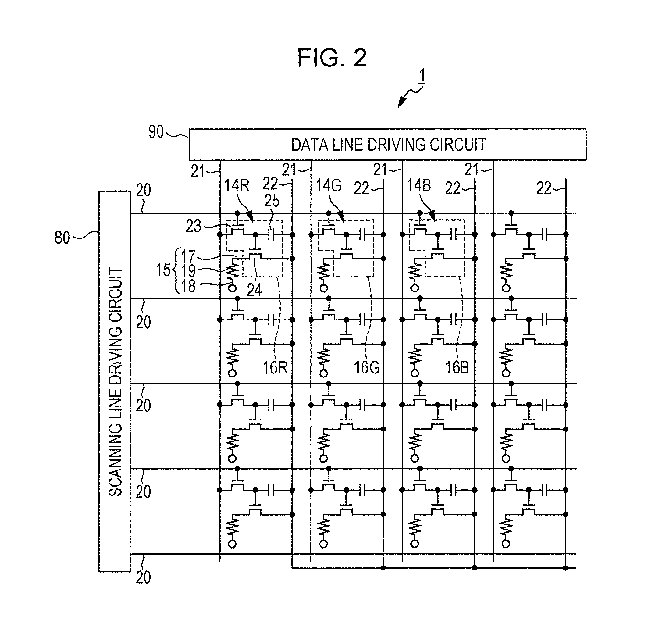
[0049]As shown in FIG. 1, the organic EL device 1 as the light emitting device of this embodiment includes a substrate 10, a display region 11 provided on a first surface of the substrate 10, and a non-display region 12 provided outside of the display region 11 (a region between the display region 11 and a circumferential edge portion of the substrate 10). A plurality of pixels 13 are disposed in a matrix pattern in the display region 11, and peripheral circuits for making the pixels emit light are provided in the non-display region. As examples of the peripheral circuits, scanning line driving circuits 80, a data line driving circuit 90, an in...

Example

Second Embodiment

[0093]FIG. 5 is a plan view illustrating light emitting elements of a light emitting device according to a second embodiment. The light emitting device according to the second embodiment will be described with reference to FIG. 5. Note that in the following description, the same constituent elements as those in the first embodiment will be given the same reference numerals and duplicate description thereof will be omitted.

[0094]In an organic EL device 101 as the light emitting device according to this embodiment, a first red sub-pixel 114R, a first green sub-pixel 114G, and a first blue sub- pixel 114B configuring a first pixel 113, and a second red sub-pixel 114′R, a second green sub-pixel 114′G, and a second blue sub-pixel 114′B configuring a second pixel 113′, are disposed line-symmetrically in the first direction (direction in which the same color sub-pixels are arranged). Light emitting elements 115 and 115′ are disposed respectively corresponding to the sub-pi...

Example

Third Embodiment

[0116]Electronic Apparatus

[0117]Next, an electronic apparatus according to a third embodiment of the invention will be described with reference to FIG. 9. FIG. 9 is a schematic perspective view illustrating a head mount display as an electronic apparatus.

[0118]As shown in FIG. 9, a head mount display 1000 as the electronic apparatus of this embodiment includes two display units 1001 that are provided corresponding to the right and left eyes. A viewer can see letters, images, and so on that are displayed on the display units 1001 by wearing the head mount display 1000 on the head like glasses. For example, the viewer can see and enjoy a three-dimensional picture when images considering parallax are displayed on the right and left display units 1001.

[0119]The organic EL device 1 described above is mounted on each of the display units 1001. Accordingly, the head mount display 1000 is an apparatus having excellent display quality with little color drift. Moreover, the he...


PUM


Abstract

An organic EL device as a light emitting device includes: a first light emitting element that is disposed on a first surface of a substrate and that has a first pixel electrode; a second light emitting element that has a second pixel electrode; and an insulating layer that is provided with a first opening which exposes the first pixel electrode and a second opening which exposes the second pixel electrode. Further, in the organic EL device, the first opening is configured so that the insulating layer covers equal to or more than 50% of the circumferential edge portion of the first pixel electrode, and the second opening is configured so that the insulating layer covers less than 50% of the circumferential edge portion of the second pixel electrode.

Description

BACKGROUND[0001]1. Technical Field[0002]The present invention relates to light emitting devices and electronic apparatuses including the stated light emitting devices.[0003]2. Related Art[0004]An active matrix EL device that includes: EL elements each sandwiching an organic electroluminescence layer between a negative electrode and a positive electrode; and transistors and capacitors for controlling the driving of the EL elements, is widely known. In such EL device, there is provided a passivation layer which has an opening at a position on the positive electrode and whose bottom end extends on the positive electrode so as to electrically insulate the adjacent positive electrodes from each other (JP-A-08-241048).[0005]It is proposed to cause light emitting areas of the EL elements that are provided corresponding to color display pixels (red, green and blue) arranged in a matrix pattern to differ in size from each other in an organic EL display apparatus that includes the EL elements...

Claims


Application Information

Patent Timeline
IPC IPC(8): H01L33/08H01L33/36
CPCH01L27/3246H01L2251/5315H01L27/32H01L27/3216H01L51/5265H01L2924/0002H01L51/52H01L33/36H01L33/08H10K59/352H10K59/122H10K50/852H10K2102/3026H01L2924/00
Inventor IWASAKI, MASANORIFUJITA, SHIN
Owner SEIKO EPSON CORP
Why Eureka
Try Eureka