
Semiconductor device, power transmission device, power reception device, charging system, wireless communication system, and charging method

a technology of power transmission device and power reception device, which is applied in the direction of electrochemical generators, secondary cell servicing/maintenance, transportation and packaging, etc., can solve the problems of power waste, power transmission device cannot detect whether or not the power reception device is present, and relationship between the power transmission device and the power reception device, so as to effectively use power to charge the battery

Active Publication Date: 2014-01-30
KK TOSHIBA
View PDF5 Cites 25 Cited by
  • Summary
  • Abstract
  • Description
  • Claims
  • Application Information

AI Technical Summary

Benefits of technology

This patent describes a semiconductor device that can transmit a wireless signal to a power reception device, and the power reception device can charge a battery using that wireless signal. The device has a control circuit and a reception circuit, and can transmit communication power or charging power depending on the response signal it receives. This technology allows for wireless charging without the need for physical contact or cables.

Problems solved by technology

In this system, the power transmission device cannot detect whether or not the power reception device is present.
Therefore, even when the power reception device is not present, the power transmission device has to radiate charging power at all times, so that the power is wasted.
Also, the power transmission device cannot obtain information of reception power limit (lower limit of power capable of charging a battery) and charge completion of the power reception device, so that the power transmission device transmits power under a predetermined certain transmission condition.
Therefore, the relationship between the power transmission device and the power reception device is usually limited to one-to-one relationship of predetermined devices.
Thus, the flexibility of the system is low.

Method used


Image

  • Semiconductor device, power transmission device, power reception device, charging system, wireless communication system, and charging method
  • Semiconductor device, power transmission device, power reception device, charging system, wireless communication system, and charging method
  • Semiconductor device, power transmission device, power reception device, charging system, wireless communication system, and charging method

Examples


first embodiment

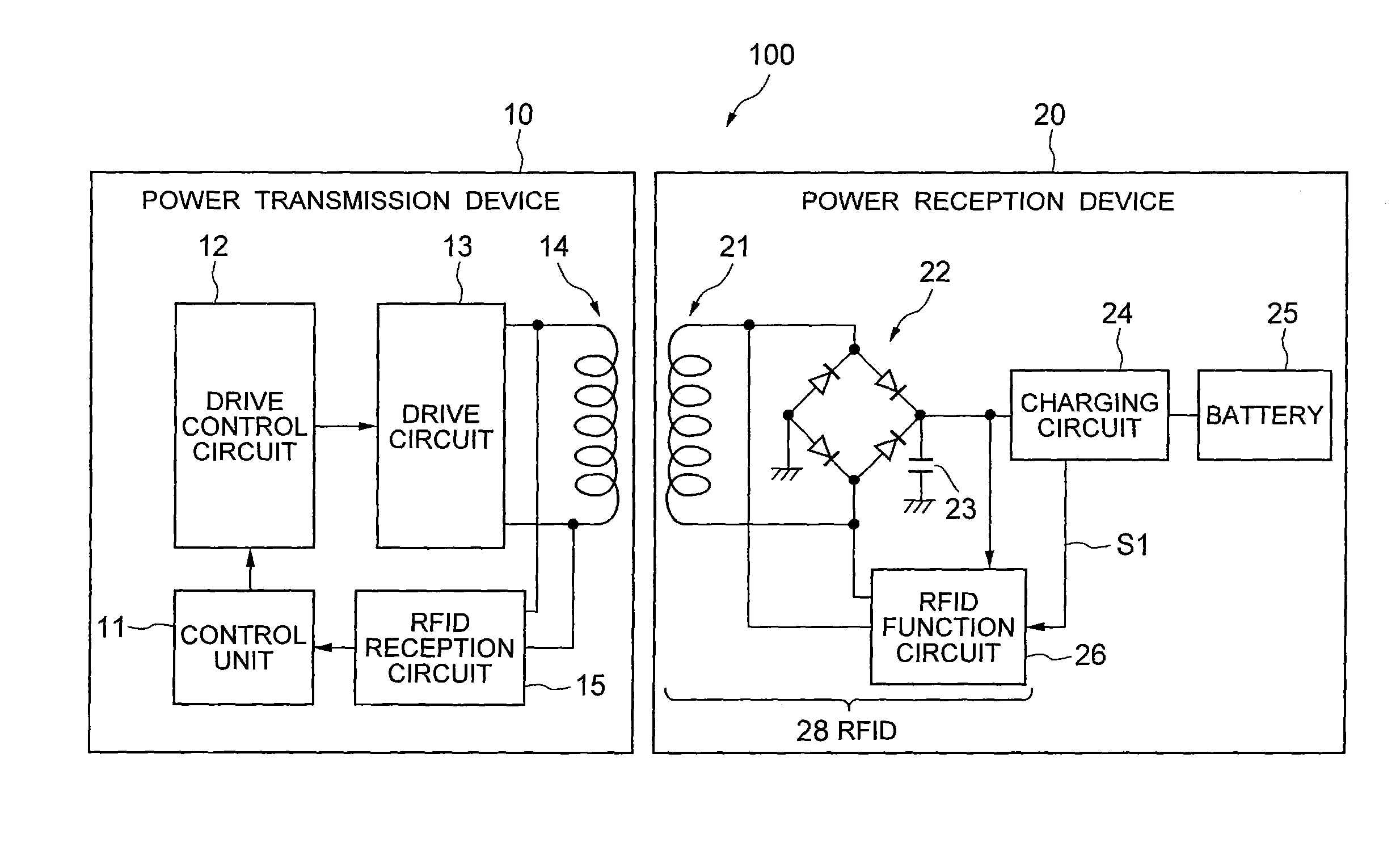
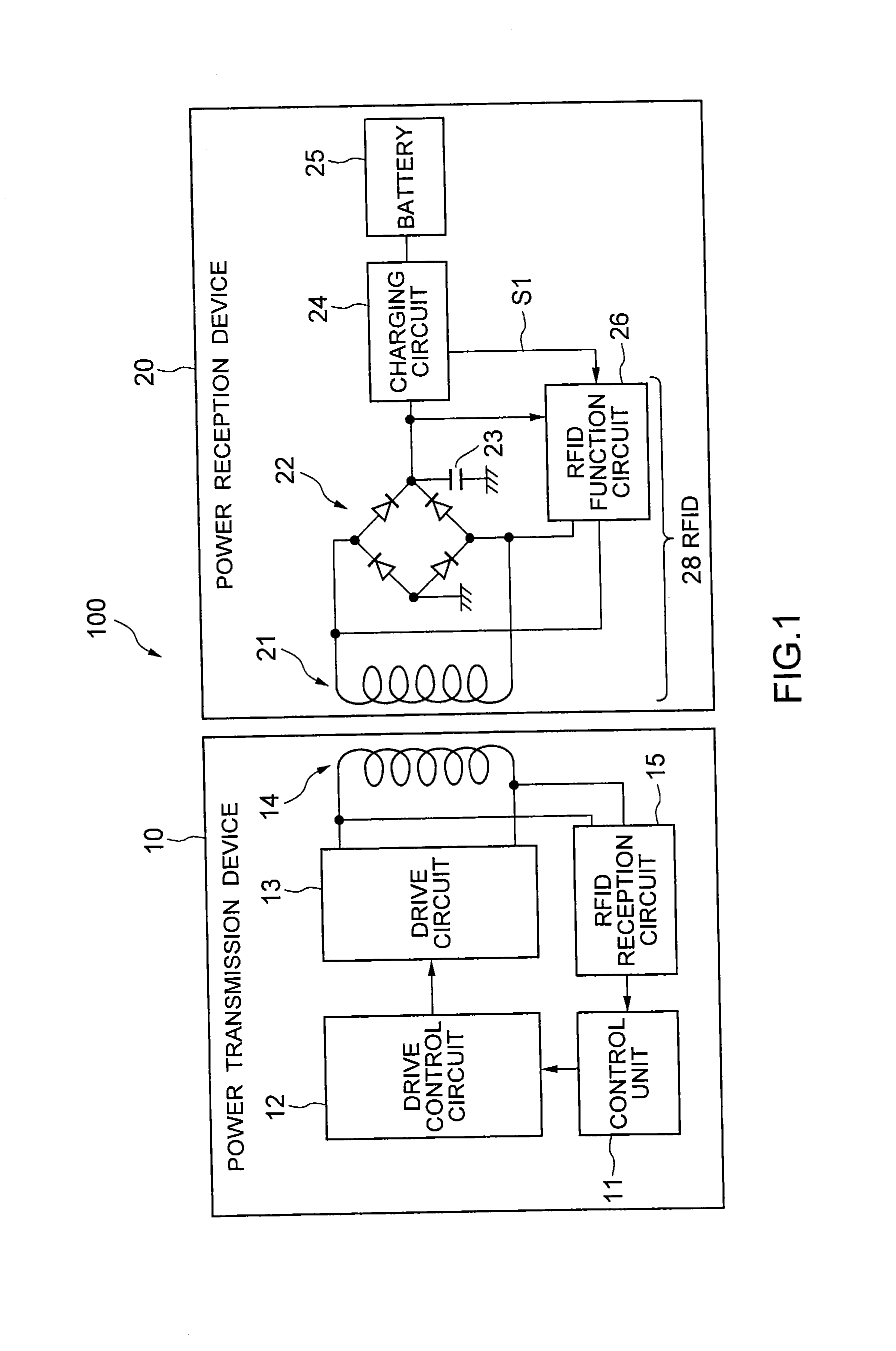
[0021]FIG. 1 is a block diagram showing a configuration of a charging system 100 according to a first embodiment of the present invention. As shown in FIG. 1, the charging system 100 (non-contact charging system) includes a power transmission device 10 and a power reception device 20.

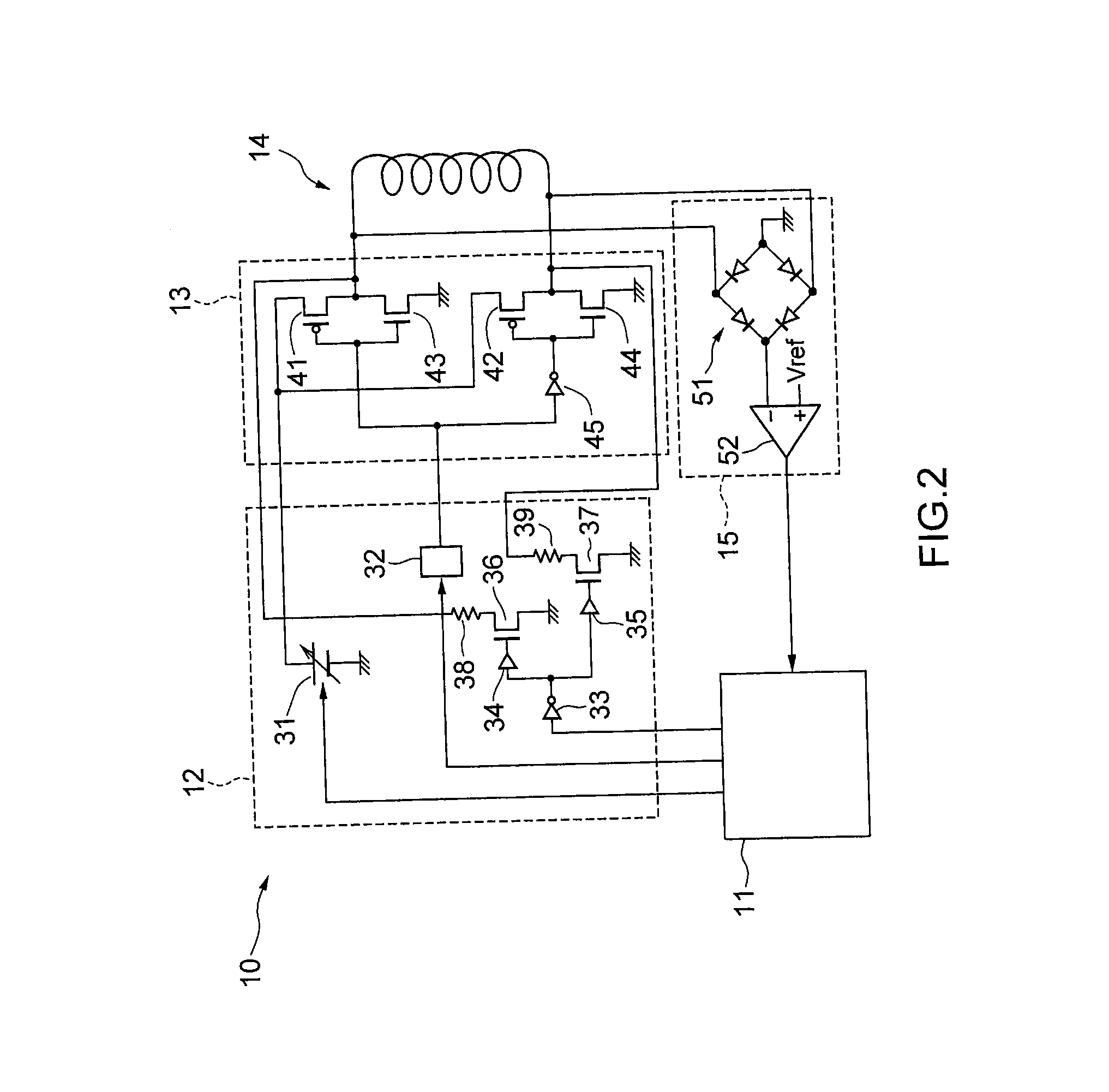
[0022]The power transmission device 10 includes a control unit (for example, CPU) 11, a drive control circuit 12, a drive circuit 13, a transmission side coil 14, and an RFID (Radio Frequency Identification) reception circuit (reception circuit) 15. Among them, for example, the control unit 11, the drive control circuit 12, and the RFID reception circuit 15 can be formed as one semiconductor device (integrated circuit).

[0023]The power reception device 20 includes a reception side coil 21, a rectifier 22, a smoothing capacitor 23, a charging circuit 24, a battery (secondary cell) 25, and an RFID function circuit 26. Among them, for example, the rectifier 22, the smoothing capacitor 23, the charging circu...

second embodiment

[0082]In a second embodiment, the RFID function circuit 26 of the power reception device 20 is operated by the power of the battery 25.

[0083]FIG. 6 is a block diagram showing a configuration of a power reception device 20 according to the second embodiment of the present invention. As shown in FIG. 6, the power reception device 20 is different from that of the first embodiment shown in FIG. 1 in a point that the power is supplied from the battery 25 to the RFID function circuit 26 while the power is not supplied from the rectifier 22 to the RFID function circuit 26. The other components are the same as those in the first embodiment shown in FIG. 1, so that the same components are denoted by the same reference numerals and the description thereof will be omitted.

[0084]In the charging system 100 that uses such a power reception device 20, the power transmission device 10 need not transmit power for operating the RFID function circuit 26 when not charging the battery 25. Therefore, the...

third embodiment

[0088]In a third embodiment, the power transmission device 10 has an RFID write function in addition to an RFID read function of the first embodiment, and the power transmission device 10 writes information to the RFID function circuit 26 of the power reception device 20.

[0089]For example, the power transmission device 10 of the present embodiment transmits a signal for writing the number of times of charging before starting the transmission of the charging power. When the power reception device 20 receives the signal for writing the number of times of charging, the power reception device 20 adds 1 to the number of times of charging stored in the memory included in the RFID function circuit 26 and stores the added number of times of charging. Thereby, when the number of times of charging exceeds a predetermined number of times, the power reception device 20 can notify a user accordingly by using a lamp, a display, or the like.

[0090]In this way, according to the present embodiment, t...


PUM


Abstract

A semiconductor device transmits a wireless signal to a power reception device that charges a battery, transmits a charge completion signal when the battery charge is completed, and transmits a response signal in reply to a query signal in the wireless signal. The semiconductor device includes a drive control circuit, a reception circuit, and a controller. The controller can control, when the reception circuit does not receive the response signal or receives the charge completion signal, the drive control circuit to transmit communication capable power that makes it possible to communicate with the power reception device and control, when the reception circuit receives the response signal and does not receive the charge completion signal, the drive control circuit to transmit charging power capable of charging the battery of the power reception device by the wireless signal, the charging power being higher than the communication capable power.

Description

CROSS REFERENCE TO RELATED APPLICATIONS[0001]This application is a Continuation application of PCT Application No. PCT / JP2012 / 050741, filed Jan. 16, 2012 and based upon and claiming the benefit of priority from prior Japanese Patent Application No. 2011-009820, filed Jan. 20, 2011, the entire contents of all of which are incorporated herein by reference.TECHNICAL FIELD[0002]The present invention relates to a semiconductor device, a power transmission device, a power reception device, a charging system, a wireless communication system, and a charging method.BACKGROUND ART[0003]A non-contact charging system is used in a handset of a home cordless phone and the like. In the non-contact charging system, a coil (inductor) is included in each of a power transmission device on the power supply side and a power reception device on the power reception side, energy (electric power) transmitted from the power transmission device is transmitted to the power reception device by mutual induction,...

Claims


Application Information

Patent Timeline
Patent Type & Authority Applications(United States)
IPC IPC(8): H02J7/02H02J7/00
CPCH02J7/025H01M10/44H01M10/46Y02T90/16Y02T90/14B60L2210/30B60L2210/40Y02T10/7072B60L53/22B60L53/122H02J2310/48H02J7/00034Y02T10/72Y02T10/70Y02E60/10H02J50/80H02J50/40H02J50/10B60L53/12H02J7/0049Y02T90/12H04B5/79
Inventor KOREKODA, HIDEAKI
Owner KK TOSHIBA
Learn More