Light-Emitting Element, Light-Emitting Device, Electronic Device, and Lighting Device

a technology of light-emitting elements and electronic devices, which is applied in the direction of luminescent compositions, thermoelectric devices, organic chemistry, etc., can solve the problems of difficult to obtain features, and achieve the effects of high reliability, high emission efficiency, and long li

Active Publication Date: 2014-02-06
SEMICON ENERGY LAB CO LTD
View PDF3 Cites 163 Cited by
  • Summary
  • Abstract
  • Description
  • Claims
  • Application Information

AI Technical Summary

Benefits of technology

[0039]One embodiment of the present invention can provide a light-emitting element having a long lifetime. By using the light-emitting element, a light-emitting device, an electronic device, and a lighting device each having high reliability can be provided. One embodiment of the

Problems solved by technology

This feature is difficult to obtain with point light sources typified by inca

Method used


Image

  • Light-Emitting Element, Light-Emitting Device, Electronic Device, and Lighting Device
  • Light-Emitting Element, Light-Emitting Device, Electronic Device, and Lighting Device
  • Light-Emitting Element, Light-Emitting Device, Electronic Device, and Lighting Device

Examples


embodiment 1

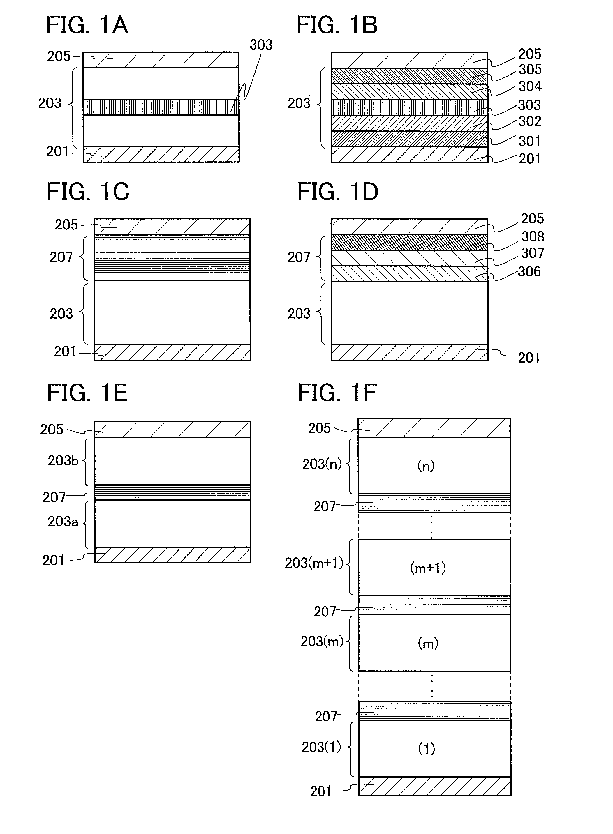
[0083]In this embodiment, light-emitting elements in one embodiment of the present invention will be described with reference to FIGS. 1A to 1F.

[0084]Light-emitting elements given in this embodiment as examples each include a pair of electrodes and a layer containing a light-emitting organic compound (EL layer) between the pair of electrodes.

[0085]A light-emitting element illustrated in FIG. 1A includes an EL layer 203 between a first electrode 201 and a second electrode 205. In this embodiment, the first electrode 201 serves as an anode, and the second electrode 205 serves as a cathode.

[0086]When a voltage higher than the threshold voltage of the light-emitting element is applied between the first electrode 201 and the second electrode 205, holes are injected to the EL layer 203 from the first electrode 201 side and electrons are injected to the EL layer 203 from the second electrode 205 side. The injected electrons and holes are recombined in the EL layer 203 and a light-emitting ...

embodiment 2

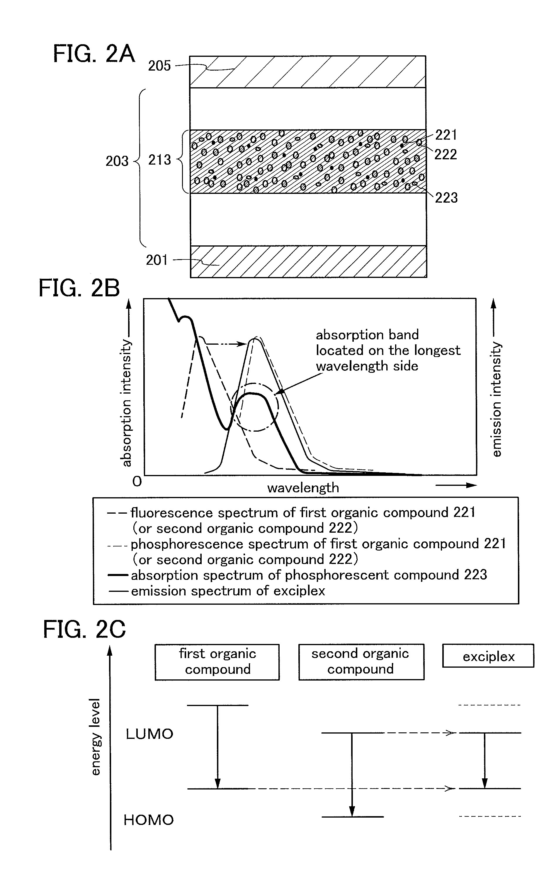
[0175]In this embodiment, a light-emitting element in one embodiment of the present invention will be described with reference to FIGS. 2A to 2C.

[0176]A light-emitting element illustrated in FIG. 2A includes an EL layer 203 between a first electrode 201 and a second electrode 205. The EL layer 203 includes a light-emitting layer 213.

[0177]In the light-emitting element illustrated in FIG. 2A, the light-emitting layer 213 contains a first organic compound 221, a second organic compound 222, and a phosphorescent compound 223. The first organic compound 221 is represented by the general formula (G0) shown in Embodiment 1 and has a molecular weight greater than or equal to 500 and less than or equal to 2000. The second organic compound 222 is a compound having an electron-transport property.

[0178]The phosphorescent compound 223 is a guest material in the light-emitting layer 213. In this embodiment, one of the first organic compound 221 and the second organic compound 222, the content of...

embodiment 3

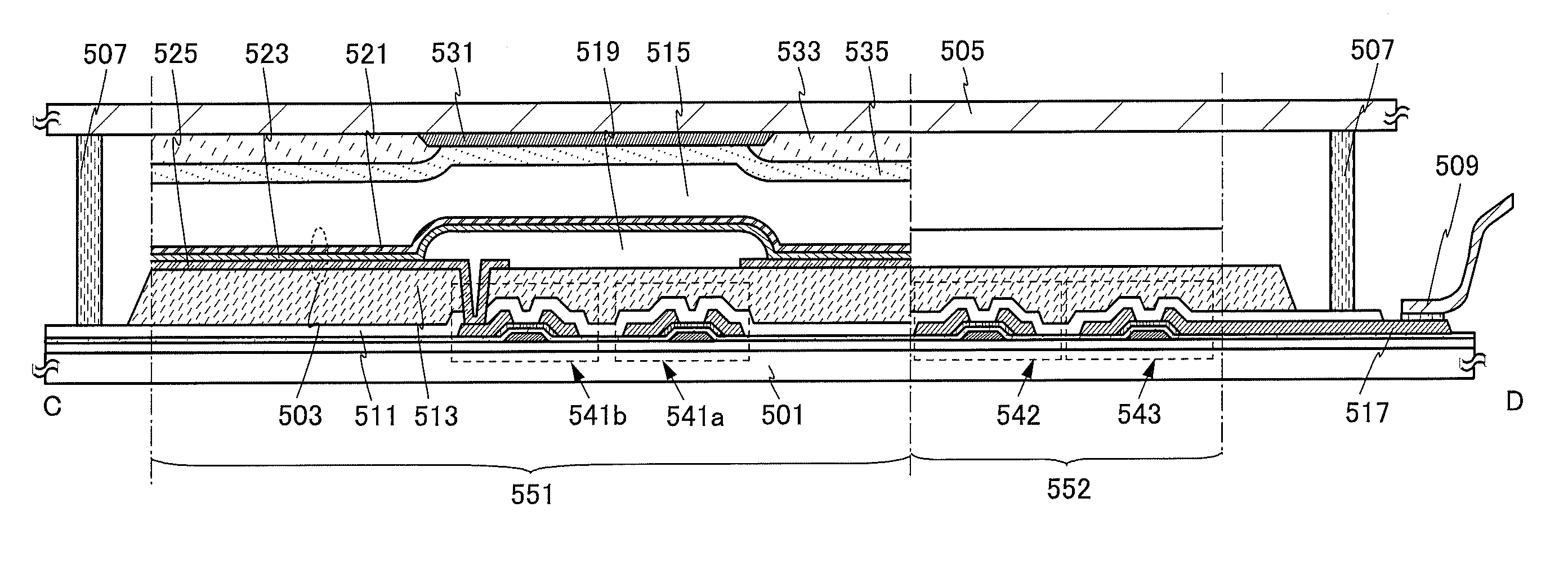
[0212]In this embodiment, a light-emitting device in one embodiment of the present invention will be described with reference to FIGS. 3A and 3B. FIG. 3A is a plan view of a light-emitting device in one embodiment of the present invention, and FIG. 3B is a cross-sectional view taken along dashed-dotted line A-B in FIG. 3A.

[0213]In the light-emitting device of this embodiment, a light-emitting element 403 (a first electrode 421, an EL layer 423, and a second electrode 425) is provided in a space 415 surrounded by a support substrate 401, a sealing substrate 405, and a sealing material 407. The light-emitting element 403 has a bottom-emission structure; specifically, the first electrode 421 which transmits visible light is provided over the support substrate 401, the EL layer 423 is provided over the first electrode 421, and the second electrode 425 which reflects visible light is provided over the EL layer 423.

[0214]As the light-emitting element 403 of this embodiment, the light-emit...


PUM


Abstract

A light-emitting element having a long lifetime is provided. A light-emitting element exhibiting high emission efficiency in a high luminance region is provided. A light-emitting element includes a light-emitting layer between a pair of electrodes. The light-emitting layer contains a first organic compound, a second organic compound, and a phosphorescent compound. The first organic compound is represented by a general formula (G0). The molecular weight of the first organic compound is greater than or equal to 500 and less than or equal to 2000. The second organic compound is a compound having an electron-transport property. In the general formula (G0), Ar1 and Ar2 each independently represent a fluorenyl group, a spirofluorenyl group, or a biphenyl group, and Ar3 represents a substituent including a carbazole skeleton.

Description

TECHNICAL FIELD[0001]The present invention relates to a light-emitting element utilizing electroluminescence (EL) (also referred to as an EL element), a light-emitting device, an electronic device, and a lighting device.BACKGROUND ART[0002]In recent years, research and development have been extensively conducted on EL elements. In a basic structure of EL elements, a layer containing a light-emitting substance is provided between a pair of electrodes. By applying voltage to this element, light emission from the light-emitting substance can be obtained.[0003]Since such an EL element is of self-light-emitting type, it is considered that the EL element has advantages over a liquid crystal display in that visibility of pixels is high, backlight is not required, and so on and is therefore suitable as flat panel display elements. In addition, it is also a great advantage that the EL element can be manufactured as a thin and lightweight element. Furthermore, very high speed response is also...

Claims


Application Information

Patent Timeline
IPC IPC(8): H01L51/50
CPCH01L51/5016C07D209/86H10K85/6572H10K50/12H10K50/11H10K2101/10H10K2101/90C09K11/025C09K11/06H10K85/631H10K85/615C09K2211/1007C09K2211/1044C09K2211/185H10K85/633H10K85/342H10K85/636H10K85/654H10K85/6576H10K50/15H10K50/16H10K85/624H10K85/626
Inventor HAMADA, TAKAOSEO, HIROMIABE, KANTATAKEDA, KYOKOSEO, SATOSHI
Owner SEMICON ENERGY LAB CO LTD
Why Eureka
Try Eureka