Semiconductor package, manufacturing method thereof, and semiconductor package manufacturing mold
- Summary
- Abstract
- Description
- Claims
- Application Information
AI Technical Summary
Benefits of technology
Problems solved by technology
Method used
Image
Examples
Embodiment Construction
[0038]Embodiments of the present invention will now be described in detail with reference to the accompanying drawings. The invention may, however, be embodied in many different forms and should not be construed as being limited to the embodiments set forth herein. Rather, these embodiments are provided so that this disclosure will be thorough and complete, and will fully convey the scope of the invention to those skilled in the art.
[0039]In the drawings, the shapes and dimensions of elements may be exaggerated for clarity, and the same reference numerals will be used throughout to designate the same or like elements.
[0040]To define terms regarding directions, an outward direction or an inward direction may be a direction toward an outer edge of a molding unit 120 from the center of the molding unit 120 or vice versa.
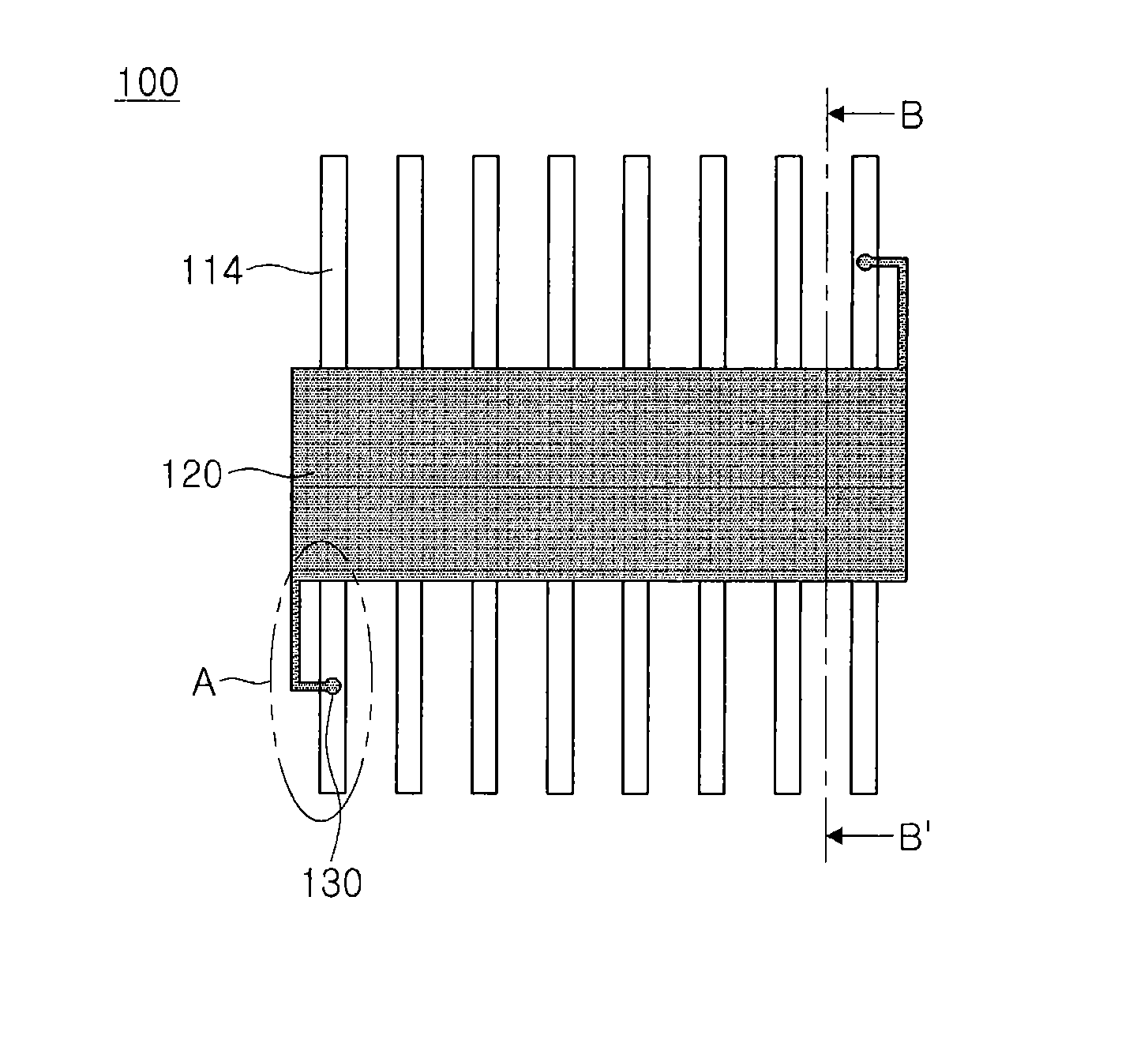
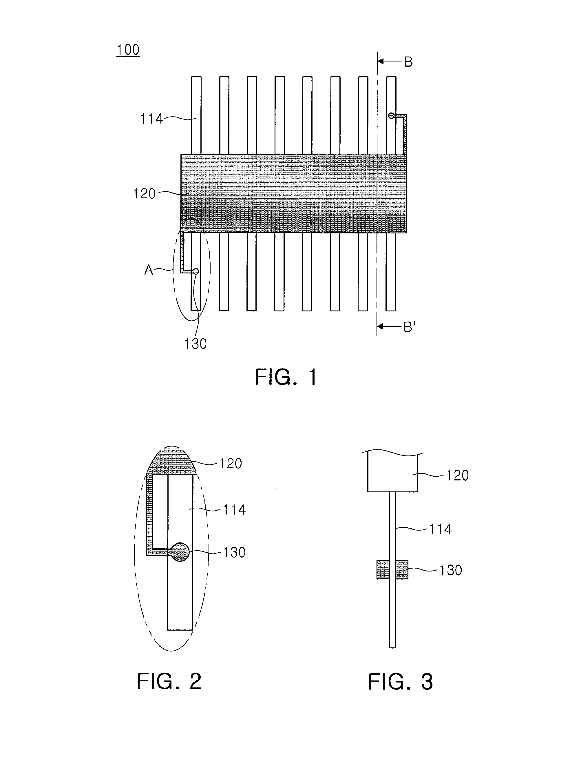
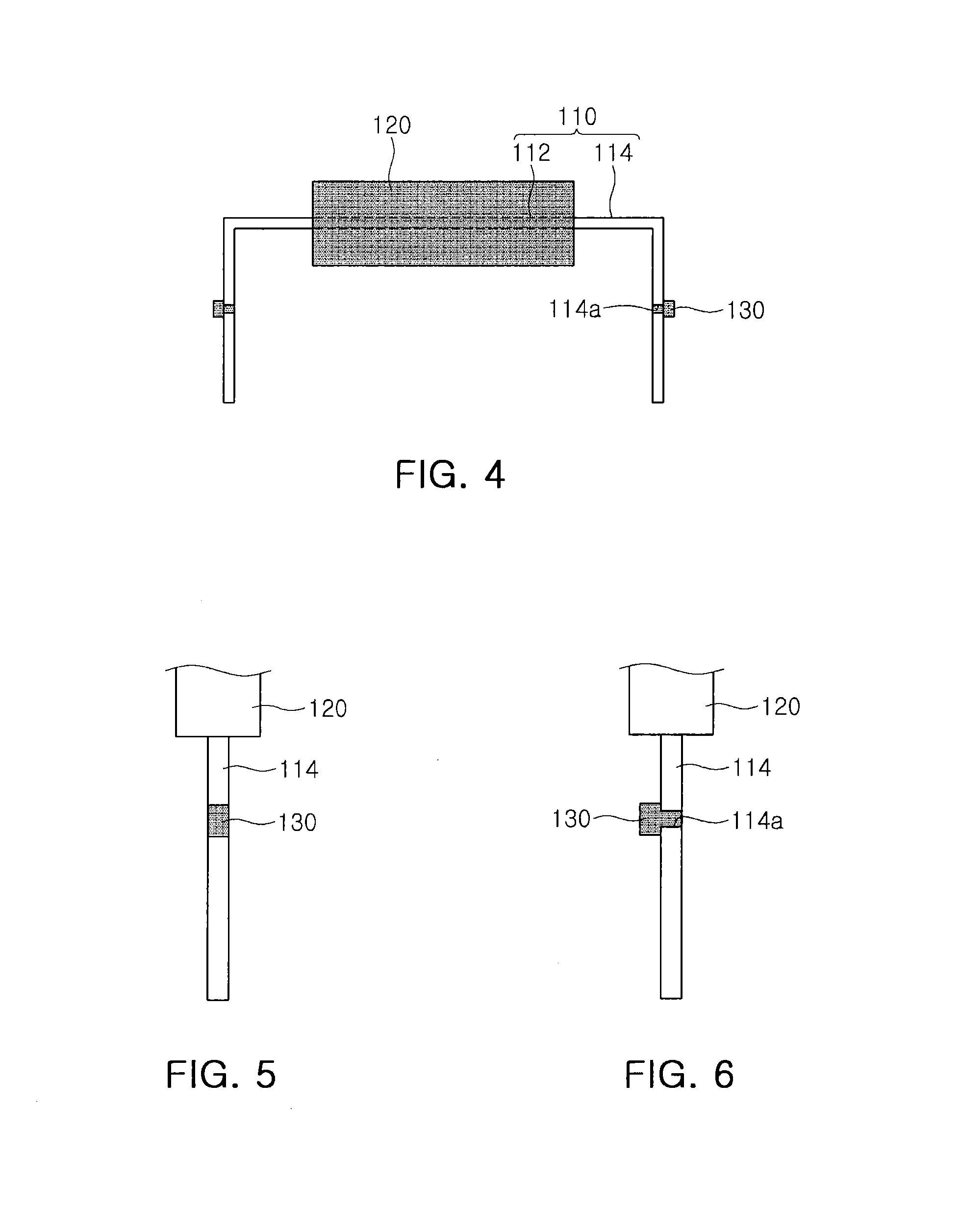
[0041]FIG. 1 is a plan view of a semiconductor package according to an embodiment of the present invention. FIG. 2 is an enlarged plan view of part A of FIG. 1. FIG. 3 ...
PUM
| Property | Measurement | Unit |
|---|---|---|
| Moldable | aaaaa | aaaaa |
Abstract
Description
Claims
Application Information
 - R&D Engineer
- R&D Manager
- IP Professional
- Industry Leading Data Capabilities
- Powerful AI technology
- Patent DNA Extraction
Browse by: Latest US Patents, China's latest patents, Technical Efficacy Thesaurus, Application Domain, Technology Topic, Popular Technical Reports.
© 2024 PatSnap. All rights reserved.Legal|Privacy policy|Modern Slavery Act Transparency Statement|Sitemap|About US| Contact US: help@patsnap.com


