
Method of manufacturing printed circuit board

Inactive Publication Date: 2014-02-13
SAMSUNG ELECTRO MECHANICS CO LTD
View PDF2 Cites 5 Cited by
  • Summary
  • Abstract
  • Description
  • Claims
  • Application Information

AI Technical Summary

Benefits of technology

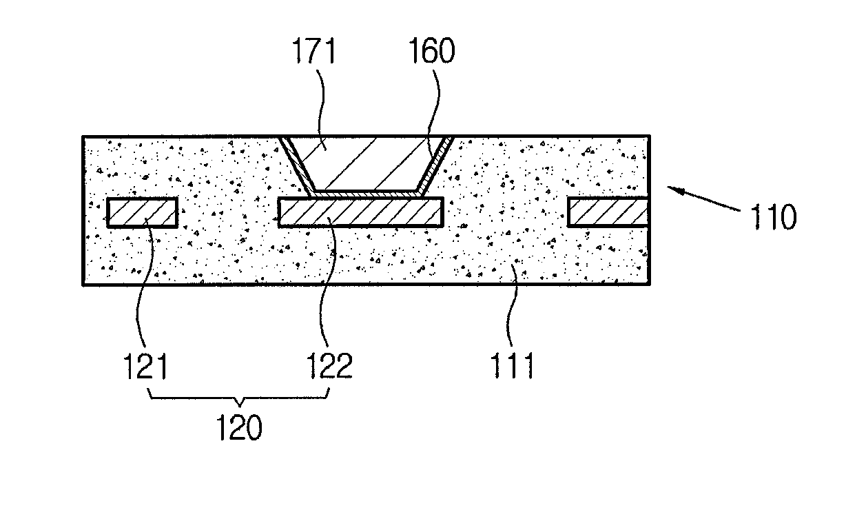
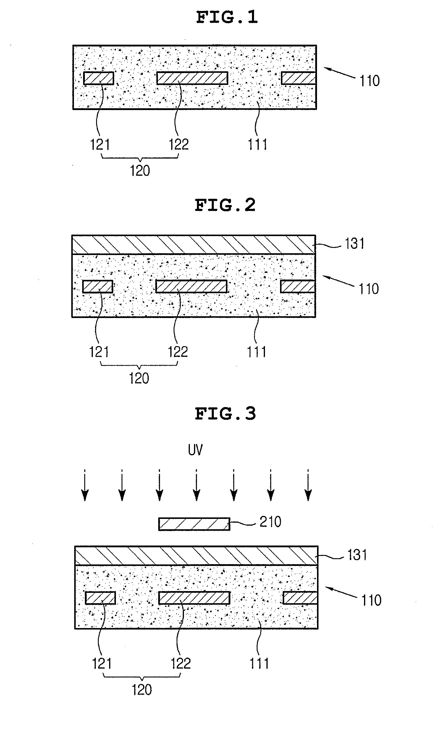
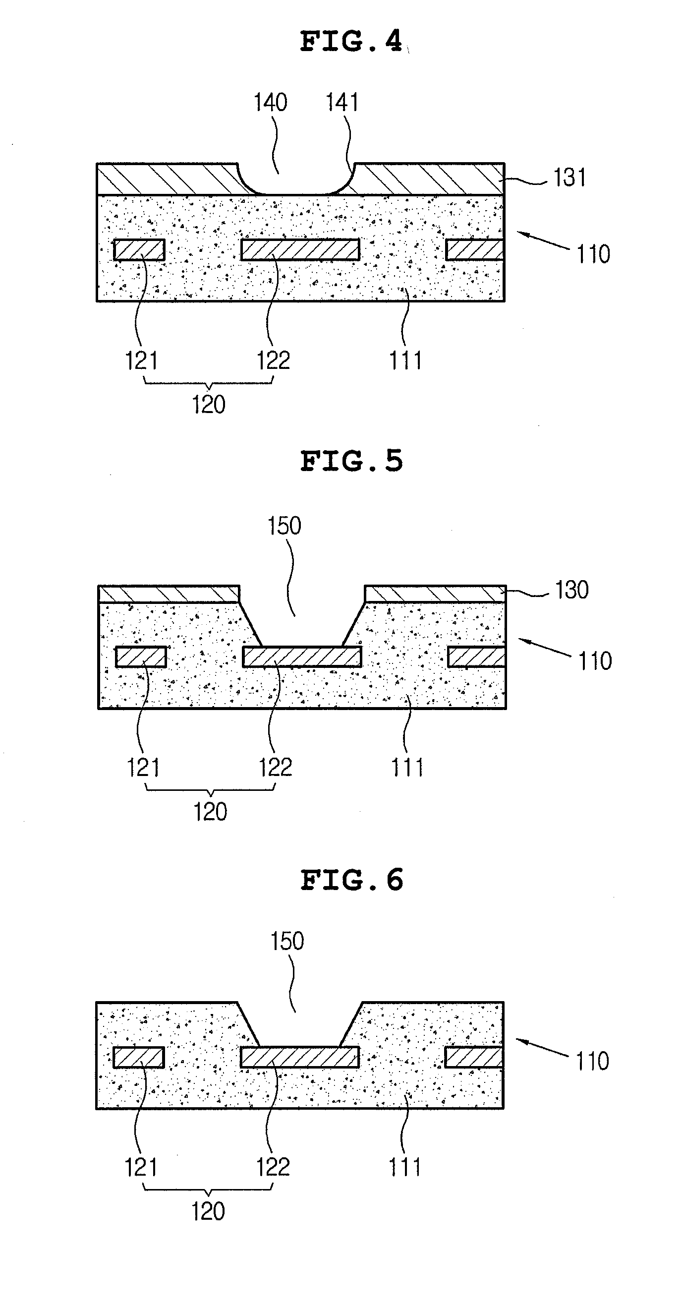
The present invention provides a method for manufacturing a printed circuit board with a via hole having a tapered shape using a plasma etching method. The method includes forming an opening part of a photosensitive resist in a foot shape, simultaneously forming multiple via holes, exposing the connection pad on the insulating layer, etching the insulating layer to expose the connection pad, and forming a via by filling the via hole. The photosensitive resist used may be a positive or negative photosensitive material, and its thickness may be controlled to control the foot shape of the opening part. The method includes curing the photosensitive resist before exposing it, and may use a mask or overexposure to form the opening part. The via hole may be formed using a plasma etching method, and the remaining photosensitive resist may be removed afterward. The technical effects of this invention include improved manufacturing efficiency and reliability of printed circuit boards with tapered via holes.

Problems solved by technology

Specification which is required for the printed circuit board having the high density and high reliability has a close relationship with that of the semiconductor chip, and there are many challenges such as miniaturization of a circuit, high electrical property, high speed signal transmission structure, high reliability, high functionality, and the like.

Method used


Image

  • Method of manufacturing printed circuit board
  • Method of manufacturing printed circuit board
  • Method of manufacturing printed circuit board

Examples


Embodiment Construction

[0029]The objects, features and advantages of the present invention will be more clearly understood from the following detailed description of the preferred embodiments taken in conjunction with the accompanying drawings. Throughout the accompanying drawings, the same reference numerals are used to designate the same or similar components, and redundant descriptions thereof are omitted. Further, in the following description, the terms “first”, “second”, “one side”, “the other side” and the like are used to differentiate a certain component from other components, but the configuration of such components should not be construed to be limited by the terms. Further, in the description of the present invention, when it is determined that the detailed description of the related art would obscure the gist of the present invention, the description thereof will be omitted.

[0030]Hereinafter, preferred embodiments of the present invention will be described in detail with reference to the attac...


PUM


Abstract

Disclosed herein is a method of manufacturing a printed circuit board, the method including: preparing a base substrate having an insulating layer and a connection pad formed in the insulating layer; forming a photosensitive resist on the insulating layer; forming an opening part of which a side surface has a foot shape by patterning the photosensitive resist; forming a via hole exposing the connection pad by etching the insulating layer exposed by the opening part; and forming a via by filling the via hole.

Description

CROSS REFERENCE TO RELATED APPLICATION[0001]This application claims the benefit of Korean Patent Application No. 10-2012-0088449, filed on Aug. 13, 2012, entitled “Method of Manufacturing a Printed Circuit Board”, which is hereby incorporated by reference in its entirety into this application.BACKGROUND OF THE INVENTION[0002]1. Technical Field[0003]The present invention relates to a method of manufacturing a printed circuit board.[0004]2. Description of the Related Art[0005]Recently, a demand for a technology of directly mounting a semiconductor chip on a printed circuit board with high density of the semiconductor chip, and high speed of signal transmission speed has become increased. Accordingly, a printed circuit board having high density and high reliability capable of implementing a high density semiconductor chip has been required to be developed.[0006]Specification which is required for the printed circuit board having the high density and high reliability has a close relatio...

Claims


Application Information

Patent Timeline
IPC IPC(8): H05K3/00H05K3/10
CPCH05K3/0079H05K3/107H05K3/0041H05K3/0082H05K3/421H05K2201/09827H05K2201/09854H05K2203/0594H05K3/0023H05K2203/0502
Inventor JUNG, JAE MOKKIM, MIN SOOSONG, HUN JUNEKIM, BA WOOL
Owner SAMSUNG ELECTRO MECHANICS CO LTD
Learn More